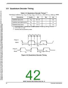
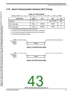
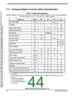
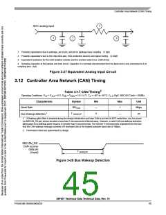
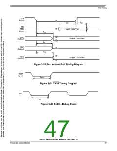
3.13 JTAG Timing
1, 3
Table 3-18 JTAG Timing
Operating Conditions: VSS = VSSA = 0 V, VDD = VDDA = 3.0–3.6 V, TA = –40° to +85°C, CL ≤ 50pF, fOP = 80MHz
Characteristic
TCK frequency of operation2
Symbol
Min
Max
Unit
fOP
DC
10
MHz
TCK cycle time
tCY
tPW
tDS
100
50
—
—
ns
ns
ns
ns
ns
ns
ns
ns
TCK clock pulse width
TMS, TDI data set-up time
TMS, TDI data hold time
TCK low to TDO data valid
TCK low to TDO tri-state
TRST assertion time
DE assertion time
0.4
1.2
—
—
tDH
—
tDV
26.6
23.5
—
tTS
—
tTRST
tDE
50
4T
—
1. Timing is both wait state and frequency dependent. For the values listed, T = clock cycle. For 80MHz operation,
T = 12.5ns.
2. TCK frequency of operation must be less than 1/8 the processor rate.
3. Parameters listed are guaranteed by design.
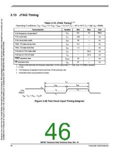
tCY
tPW
tPW
VIH
VM
VM
TCK
(Input)
VIL
VM = VIL + (VIH – VIL)/2
Figure 3-29 Test Clock Input Timing Diagram
56F807 Technical Data Technical Data, Rev. 16
46
Freescale Semiconductor

 FREESCALE [ Freescale ]