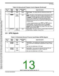
GPIO Signals
Table 2-9 Interrupt and Program Control Signals (Continued)
No. of
Pins
Signal
Name
Signal
Type
State During
Reset
Signal Description
1
RSTO
Output
Output
Reset Output—This output reflects the internal reset state of the
chip.
1
RESET
Input
(Schmitt)
Input
Reset—This input is a direct hardware reset on the processor. When
RESET is asserted low, the device is initialized and placed in the
Reset state. A Schmitt trigger input is used for noise immunity. When
the RESET pin is deasserted, the initial chip operating mode is
latched from the EXTBOOT pin. The internal reset signal will be
deasserted synchronous with the internal clocks, after a fixed number
of internal clocks.
To ensure complete hardware reset, RESET and TRST should be
asserted together. The only exception occurs in a debugging
environment when a hardware device reset is required and it is
necessary not to reset the OnCE/JTAG module. In this case, assert
RESET, but do not assert TRST.
1
EXTBOOT
Input
Input
External Boot—This input is tied to VDD to force device to boot from
(Schmitt)
off-chip memory. Otherwise, it is tied to VSS.
2.6 GPIO Signals
Table 2-10 Dedicated General Purpose Input/Output (GPIO) Signals
No.of
Pins
Signal
Name
Signal
Type
State During
Reset
Signal Description
8
GPIOB0-
GPIOB7
Input
or
Output
Input
Port B GPIO—These eight pins are dedicated General Purpose I/O
(GPIO) pins that can individually be programmed as input or output
pins.
After reset, the default state is GPIO input.
6
GPIOD0-
GPIOD5
Input
or
Input
Port D GPIO—These six pins are dedicated GPIO pins that can
individually be programmed as an input or output pins.
Output
After reset, the default state is GPIO input.
56F807 Technical Data Technical Data, Rev. 16
Freescale Semiconductor
13

 FREESCALE [ Freescale ]