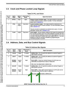
Clock and Phase Locked Loop Signals
2.3 Clock and Phase Locked Loop Signals
Table 2-5 PLL and Clock
No. of
Pins
Signal
Name
Signal
Type
State During
Reset
Signal Description
1
EXTAL
Input
Input
External Crystal Oscillator Input—This input should be connected to
an 8MHz external crystal or ceramic resonator. For more information,
please refer to Section 3.4.
1
XTAL
Input/
Output
Chip-driven
Crystal Oscillator Output—This output should be connected to an
8MHz external crystal or ceramic resonator. For more information, please
refer to Section 3.4.
This pin can also be connected to an external clock source. For more
information, please refer to Section 3.4.2.
1
CLKO
Output
Chip-driven
Clock Output—This pin outputs a buffered clock signal. By programming
the CLKOSEL[4:0] bits in the CLKO Select Register (CLKOSR), the user
can select between outputting a version of the signal applied to XTAL and
a version of the device’s master clock at the output of the PLL. The clock
frequency on this pin can also be disabled by programming the
CLKOSEL[4:0] bits in CLKOSR.
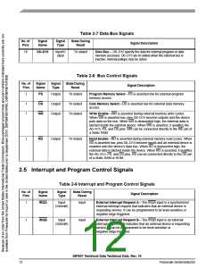
2.4 Address, Data, and Bus Control Signals
Table 2-6 Address Bus Signals
No. of
Pins
Signal
Name
Signal
Type
State During
Reset
Signal Description
6
A0–A5
Output
Tri-stated
Address Bus—A0–A5 specify the address for external Program or
Data memory accesses.
2
A6–A7
Output
Tri-stated
Address Bus—A6–A7 specify the address for external Program or
Data memory accesses.
GPIOE2-
GPIOE3
Input/O
utput
Input
Port E GPIO—These two General Purpose I/O (GPIO) pins can
individually be programmed as input or output pins.
After reset, the default state is Address Bus.
8
A8–A15
Output
Tri-stated
Input
Address Bus—A8–A15 specify the address for external Program or
Data memory accesses.
GPIOA0-
GPIOA7
Input/O
utput
Port A GPIO—These eight General Purpose I/O (GPIO) pins can be
individually programmed as input or output pins.
After reset, the default state is Address Bus.
56F807 Technical Data Technical Data, Rev. 16
Freescale Semiconductor
11

 FREESCALE [ Freescale ]