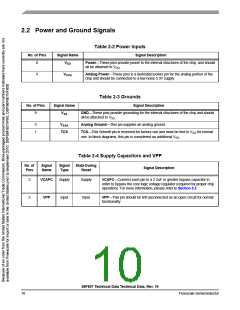
2.2 Power and Ground Signals
Table 2-2 Power Inputs
No. of Pins
Signal Name
VDD
Signal Description
8
Power—These pins provide power to the internal structures of the chip, and should
all be attached to VDD.
3
VDDA
Analog Power—These pins is a dedicated power pin for the analog portion of the
chip and should be connected to a low noise 3.3V supply.
Table 2-3 Grounds
No. of Pins
Signal Name
VSS
Signal Description
9
GND—These pins provide grounding for the internal structures of the chip and should
all be attached to VSS.
3
1
VSSA
TCS
Analog Ground—This pin supplies an analog ground.
TCS—This Schmitt pin is reserved for factory use and must be tied to VSS for normal
use. In block diagrams, this pin is considered an additional VSS.
Table 2-4 Supply Capacitors and VPP
No. of
Pins
Signal
Name
Signal
Type
State During
Reset
Signal Description
2
VCAPC
Supply
Supply
VCAPC—Connect each pin to a 2.2uF or greater bypass capacitor in
order to bypass the core logic voltage regulator (required for proper chip
operation). For more information, please refer to Section 5.2
2
VPP
Input
Input
VPP—This pin should be left unconnected as an open circuit for normal
functionality.
56F807 Technical Data Technical Data, Rev. 16
10
Freescale Semiconductor

 FREESCALE [ Freescale ]