Part 2 Signal/Connection Descriptions
2.1 Introduction
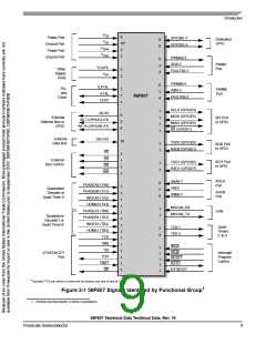
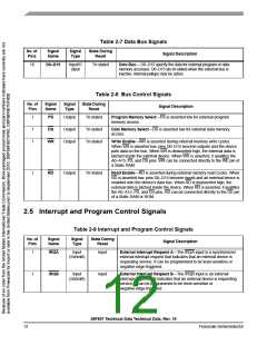
The input and output signals of the 56F807 are organized into functional groups, as shown in Table 2-1
and as illustrated in Figure 2-1. In Table 2-2 through Table 2-19, each table row describes the signal or
signals present on a pin.
Table 2-1 Functional Group Pin Allocations
Number of
Pins
Detailed
Description
Functional Group
Power (VDD or VDDA
)
11
13
4
Table 2-2
Table 2-3
Table 2-4
Ground (VSS or VSSA
)
Supply Capacitors & VPP
PLL and Clock
3
Table 2-5
Table 2-6
Address Bus1
16
Data Bus
16
4
Table 2-7
Table 2-8
Table 2-9
Table 2-10
Table 2-11
Table 2-12
Bus Control
Interrupt and Program Control
Dedicated General Purpose Input/Output
Pulse Width Modulator (PWM) Ports
5
14
26
4
Serial Peripheral Interface (SPI) Port1
Quadrature Decoder Ports2
8
4
Table 2-13
Table 2-15
Serial Communications Interface (SCI) Ports1
CAN Port
2
20
6
Table 2-16
Table 2-17
Table 2-18
Table 2-19
Analog to Digital Converter (ADC) Ports
Quad Timer Module Ports
JTAG/On-Chip Emulation (OnCE)
1. Alternately, GPIO pins
6
2. Alternately, Quad Timer pins
56F807 Technical Data Technical Data, Rev. 16
8
Freescale Semiconductor

 FREESCALE [ Freescale ]