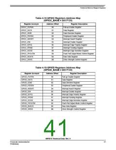
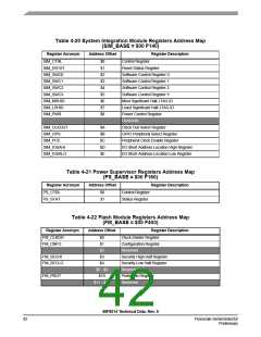
Table 4-20 System Integration Module Registers Address Map
(SIM_BASE = $00 F140)
Register Acronym
Address Offset
Register Description
SIM_CTRL
SIM_RSTAT
SIM_SWC0
SIM_SWC1
SIM_SWC2
SIM_SWC3
SIM_MSHID
SIM_LSHID
SIM_PWR
$0
$1
$2
$3
$4
$5
$6
$7
$8
Control Register
Reset Status Register
Software Control Register 0
Software Control Register 1
Software Control Register 2
Software Control Register 3
Most Significant Half JTAG ID
Least Significant Half JTAG ID
Power Control Register
Reserved
SIM_CLKOUT
SIM_GPS
$A
$B
$C
$D
$E
Clock Out Select Register
GPIO Peripheral Select Register
Peripheral Clock Enable Register
I/O Short Address Location High Register
I/O Short Address Location Low Register
SIM_PCE
SIM_IOSAHI
SIM_IOSALO
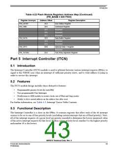
Table 4-21 Power Supervisor Registers Address Map
(PS_BASE = $00 F160)
Register Acronym
Address Offset
Register Description
PS_CTRL
PS_STAT
$0
$1
Control Register
Status Register
Table 4-22 Flash Module Registers Address Map
(FM_BASE = $00 F400)
Register Acronym
Address Offset
Register Description
Clock Divider Register
FM_CLKDIV
FM_CNFG
$0
$1
Configuration Register
Reserved
$2
FM_SECHI
FM_SECLO
$3
Security High Half Register
Security Low Half Register
Reserved
$4
$5 - $9
$10
FM_PROT
Protection Register
Reserved
$11 - $12
56F8014 Technical Data, Rev. 9
42
Freescale Semiconductor
Preliminary

 FREESCALE [ Freescale ]