JTAG Timing
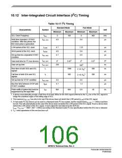
SDA
SCL
t
SU; DAT
t
t
t
SP
t
BUF
HD; STA
LOW
t
t
t
SU; STA
HD; STA
SU; STO
S
BR
P
S
t
t
HIGH
HD; DAT
2
Figure 10-14 Timing Definition for Fast and Standard Mode Devices on the I C Bus
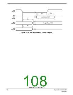
10.13 JTAG Timing
Table 10-18 JTAG Timing
Characteristic
Symbol
Min
DC
50
5
Max
Unit
MHz
ns
See Figure
10-15
TCK frequency of operation1
TCK clock pulse width
fOP
SYS_CLK/8
tPW
tDS
tDH
tDV
tTS
—
—
—
30
30
10-15
TMS, TDI data set-up time
TMS, TDI data hold time
TCK low to TDO data valid
TCK low to TDO tri-state
ns
10-16
5
ns
10-16
—
—
ns
10-16
ns
10-16
1. TCK frequency of operation must be less than 1/8 the processor rate.
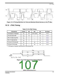
1/fOP
tPW
tPW
VIH
VM
VM
TCK
(Input)
VIL
VM = VIL + (VIH – VIL)/2
Figure 10-15 Test Clock Input Timing Diagram
56F8014 Technical Data, Rev. 9
Freescale Semiconductor
Preliminary
107

 FREESCALE [ Freescale ]