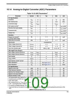
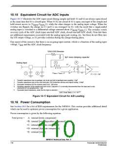
10.15 Equivalent Circuit for ADC Inputs
Figure 10-17 illustrates the ADC input circuit during sample and hold. S1 and S2 are always open/closed
at the same time that S3 is closed/open. When S1/S2 are closed & S3 is open, one input of the sample and
hold circuit moves to (V
-V
)/2, while the other charges to the analog input voltage. When the
REFH REFL
switches are flipped, the charge on C1 and C2 are averaged via S3, with the result that a single-ended
analog input is switched to a differential voltage centered about (V -V )/2. The switches switch
REFH REFL
on every cycle of the ADC clock (open one-half ADC clock, closed one-half ADC clock). Note that there
are additional capacitances associated with the analog input pad, routing, etc., but these do not filter into
the S/H output voltage, as S1 provides isolation during the charge-sharing phase.
One aspect of this circuit is that there is an on-going input current, which is a function of the analog input
voltage, V
and the ADC clock frequency.
REF
125Ω ESD Resistor
8pF noise damping capacitor
4
3
Analog Input
S1
C1
S/H
S3
C2
S2
(VREFH- VREFL )/ 2
2
1
C1 = C2 = 1pF
1. Parasitic capacitance due to package, pin-to-pin and pin-to-package base coupling; 1.8pF
2. Parasitic capacitance due to the chip bond pad, ESD protection devices and signal routing; 2.04pF
3. Equivalent resistance for the channel select mux; 100 ohms
4. Sampling capacitor at the sample and hold circuit. Capacitor C1 is normally disconnected from the input and is only
connected to it at sampling time; 1.4pf
1
5. Equivalent input impedance, when the the input is selected =
(ADC Clock Rate) x 1.4 x 10⁻¹²
Figure 10-17 Equivalent Circuit for A/D Loading
10.16 Power Consumption
See Section 10.1 for a list of IDD requirements for the 56F8014. This section provides additional detail
which can be used to optimize power consumption for a given application.
Power consumption is given by the following equation:
Total power = A: internal [static component]
+B: internal [state-dependent component]
+C: internal [dynamic component]
+D: external [dynamic component]
+E: external [static]
56F8014 Technical Data, Rev. 9
110
Freescale Semiconductor
Preliminary

 FREESCALE [ Freescale ]