Serial Communication Interface (SCI) Timing
10.11 Serial Communication Interface (SCI) Timing
1
Table 10-16 SCI Timing
Characteristic
Symbol
Min
—
Max
Unit
See Figure
—
Baud Rate2
BR
(fMAX/16)
Mbps
RXD3 Pulse Width
TXD4 Pulse Width
RXDPW
TXDPW
0.965/BR
1.04/BR
1.04/BR
ns
ns
10-12
0.965/BR
10-13
LIN Slave Mode
Deviation of slave node clock from
nominal clock rate before
synchronization
FTOL_UNSYN
-14
-2
14
2
%
%
CH
Deviation of slave node clock relative to
the master node clock after
synchronization
FTOL_SYNCH
Minimum break character length
TBREAK
13
11
Master
node bit
periods
Slavenode
bit periods
1. Parameters listed are guaranteed by design.
2. f
is the frequency of operation of the system clock in MHz, which is 32MHz for the 56F8014 device.
MAX
3. The RXD pin in SCI0 is named RXD0 and the RXD pin in SCI1 is named RXD1.
4. The TXD pin in SCI0 is named TXD0 and the TXD pin in SCI1 is named TXD1.
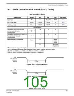
RXD
SCI receive
data pin
RXDPW
(Input)
Figure 10-12 RXD Pulse Width
TXD
SCI receive
data pin
TXDPW
(Input)
Figure 10-13 TXD Pulse Width
56F8014 Technical Data, Rev. 9
Freescale Semiconductor
Preliminary
105

 FREESCALE [ Freescale ]