2
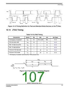
10.12 Inter-Integrated Circuit Interface (I C) Timing
2
Table 10-17 I C Timing
Standard Mode
Minimum Maximum
Fast Mode
Characteristic
Symbol
Unit
Minimum
Maximum
SCL Clock Frequency
fSCL
0
100
0
400
kHz
Hold time (repeated ) START
condition. After this period, the
first clock pulse is generated.
tHD; STA
4.0
0.6
μs
LOW period of the SCL clock
HIGH period of the SCL clock
tLOW
tHIGH
4.7
4.0
4.7
1.25
0.6
μs
μs
μs
Set-up time for a repeated START
condition
tSU; STA
0.6
Data hold time for I2C bus devices
Data set-up time
01
3.452
01
0.92
tHD; DAT
tSU; DAT
tr
μs
ns
ns
1003
250
4
Rise time of both SDA and SCL
signals
1000
300
300
300
2 +0.1Cb
4
Fall time of both SDA and SCL
signals
tf
ns
2 +0.1Cb
Set-up time for STOP condition
tSU; STO
tBUF
4.0
4.7
0.6
1.3
μs
μs
Bus free time between STOP and
START condition
Pulse width of spikes that must be
suppressed by the input filter
tSP
N/A
N/A
0.0
50
ns
1. A device must internally provide a hold time of at least 300ns for the SDA signal (referred to the V min of the SCL signal) to
IH
bridge the undefined region of the falling edge of SCL.
2. The maximum t
has only to be met if the device does not stretch the LOW period (t
) of the SCL signal.
HD; DAT
LOW
2
2
3. A Fast mode I C bus device can be used in a Standard mode I C bus system, but the requirement t
> = 250ns must then
SU; DAT
be met. This will automatically be the case if the device does not stretch the LOW period of the SCL signal. If such a device does
stretch the LOW period of the SCL signal, it must output the next data bit to the SDA line
2
t
+ t
= 1000 + 250 = 1250ns (according to the Standard mode I C bus specification) before the SCL line is released.
rmax
SU; DAT
4. C = total capacitance of the one bus line in pF.
b
56F8014 Technical Data, Rev. 9
106
Freescale Semiconductor
Preliminary

 FREESCALE [ Freescale ]