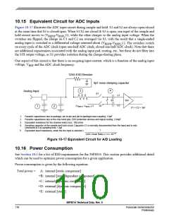
Power Consumption
A, the internal [static component], is comprised of the DC bias currents for the oscillator, leakage currents,
PLL, and voltage references. These sources operate independently of processor state or operating
frequency.
B, the internal [state-dependent component], reflects the supply current required by certain on-chip
resources only when those resources are in use. These include RAM, Flash memory and the ADCs.
2
C, the internal [dynamic component], is classic C*V *F CMOS power dissipation corresponding to the
56800E core and standard cell logic.
D, the external [dynamic component], reflects power dissipated on-chip as a result of capacitive loading
2
on the external pins of the chip. This is also commonly described as C*V *F, although simulations on two
of the I/O cell types used on the 56800E reveal that the power-versus-load curve does have a non-zero
Y-intercept.
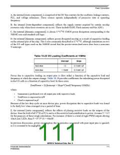
Table 10-20 I/O Loading Coefficients at 10MHz
Intercept
Slope
8mA drive
4mA drive
1.3
0.11mW / pF
0.11mW / pF
1.15mW
Power due to capacitive loading on output pins is (first order) a function of the capacitive load and
frequency at which the outputs change. Table 10-20 provides coefficients for calculating power dissipated
in the I/O cells as a function of capacitive load. In these cases:
TotalPower = Σ((Intercept + Slope*Cload)*frequency/10MHz)
where:
•
•
•
Summation is performed over all output pins with capacitive loads
TotalPower is expressed in mW
Cload is expressed in pF
Because of the low duty cycle on most device pins, power dissipation due to capacitive loads was found
to be fairly low when averaged over a period of time.
E, the external [static component], reflects the effects of placing resistive loads on the outputs of the
2
device. Sum the total of all V /R or IV to arrive at the resistive load contribution to power. Assume V = 0.5
for the purposes of these rough calculations. For instance, if there is a total of eight PWM outputs driving
10mA into LEDs, then P = 8*.5*.01 = 40mW.
In previous discussions, power consumption due to parasitics associated with pure input pins is ignored,
as it is assumed to be negligible.
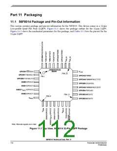
56F8014 Technical Data, Rev. 9
Freescale Semiconductor
Preliminary
111

 FREESCALE [ Freescale ]