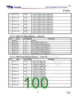
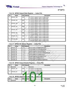
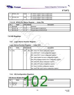
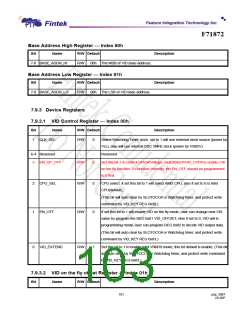
F71872
Reserved
7-6 Reserved
5-0
-
-
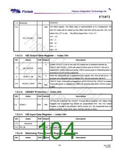
VID offset register. The offset value is representative in 2’s complement. The
00h
real VID value will be added by this offset and then will be put into VID_OUT
(when EN_OTF is set). The offset ranges from -16 to +31.
1Fh : +31.
01h : +1.
00h : +0.
3Fh : -1.
30h : -16.
VID_OFFSET
R/W
7.9.3.3 VID Output Data Register Index 02h
Bit
Name
R/W Default
Description
Enable VIDOUT. If set to one and VID output key is asserted referred as
VIDKEY, the VIDOUT_DATA will output to these pins of VIDOUT. This bit is
supplied by VSB3V and reset by the VSB3V power good or Watchdog timer is
asserted or SLOTOCC# is asserted.
0
7
EN_VIDOUT
R/W
When the sequential key is programmed to register 22H. this bit will set to 1. if
program exit sequential key to register 22H, this bit read back will be 0
VIDOUT Data. These bits is mapping to VIDOUT[5:0] if EN_VIDOUT is enable.
These bits power is supplied by VSB3V for keeping data when VDD3V power
is lose.
0
6
VIDKEY_OK
RO
5-0
VIDOUT_DATA
R/W
00h
7.9.3.4 VIDKEY Protection Index 03h
Bit
Name
R/W Default
Description
VID Key for protection the VIDOUT. If would like to program VID Output Data
Register, the sequential key should be programmed first. The VID Output
Register is disable in the default (VSB3V power on). The sequential keys are
defined as 0x32, 0x5d, 0x42, 0xac. And the exit key is 0x35.
7-0
VIDKEY
R/W
00h
7.9.3.5 VID Input Data Register Index 04h
Bit
Name
R/W Default
Description
Reserved
XXh VID Input data.
7-6
Reserved
-
-
5-0 VID_IN
R
7.9.3.6 Watchdog Timer Control Register Index 05h
Bit
Name
R/W Default
Description
102
July, 2007
V0.28P

 FINTEK [ FEATURE INTEGRATION TECHNOLOGY INC. ]