F71872
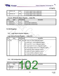
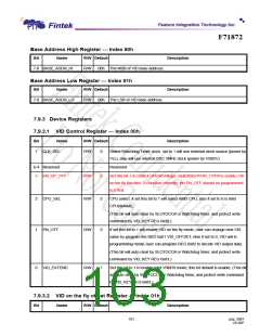
Base Address High Register Index 60h
Bit
Name
R/W Default
Description
Description
7-0 BASE_ADDR_HI
R/W 00h The MSB of VID base address.
Base Address Low Register Index 61h
Bit
Name
R/W Default
7-0 BASE_ADDR_LO
R/W 00h The LSB of VID base address.
7.9.3 Device Registers
7.9.3.1 VID Control Register Index 00h
Bit
Name
CLK_SEL
R/W Default
Description
7
R/W
0
Select Watchdog Timer clock, set to 1 will use external clock source (power by
Vcc), else will use internal OSC 2MHz clock (power by VSB3V).
6-4 Reserved
-
-
Reserved
3
EN_GP_OTF
R/W
0
Set this bit 1 to control GPIO4/Voltage_fault2/BEEP/VID_OTF# to enable VID
on the fly function. To function correctly, the EN_OTF should be programmed
to 0 first.
2
CPU_SEL
EN_OTF
R/W
R/W
0
0
CPU select, if set this bit to 1 will select AMD CPU, else if set to 0 is Intel
CPU(default),
(This bit will auto clear by SLOTOCC# or Watchdog timer, and protect write
command by VID_KEY REG 0x30.)
1
0
If set this bit to 1 will enable VID on the fly mode, user can change new VID
value by program the REG 0x01 VID_OFFSET, else if set to 0, VID will in
programming mode, user can program REG 0x02 to decide VID output data.
(This bit will auto clear by SLOTOCC# or Watchdog timer, and protect write
command by VID_KEY REG 0x03.)
VID_EXTEND
R/W
1
Set this bit to 1 to enable Intel VRM10 mode, this bit default is enable, (This bit
will auto clear by SLOTOCC# or Watchdog timer, and protect write command
by VID_KEY REG 0x03.)
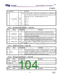
7.9.3.2 VID on the fly offset Register Index 01h
Bit
Name
R/W Default
Description
101
July, 2007
V0.28P

 FINTEK [ FEATURE INTEGRATION TECHNOLOGY INC. ]