F71872
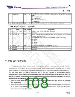
The ACPI Control the PSON_N to always on or always off or keep last
2-1 PWRCTRL
R/W
11
0
state
00 : keep last state
10 : Always on
01 : Reserved (always on)
11: Always off
When VSB 3V comes, it will set to 1, and write 1 to clear it
0
VSB_PWR_LOSS R/W
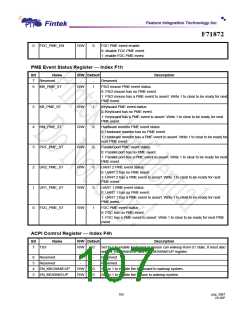
ACPI Control Register Index F5h
Bit
7
Name
SOFT_RST_ACPI
Reserved
R/W Default
Description
Software Reset to ACPI (auto clear after reset)
Reserved
R/W
-
0
-
6
5
RSTCON_EN
R/W
1
Set to 1 to enable RSTCON_EN to PCIRST, set to 0 to enable RSTCON_EN to
PWOKIN1 and PWOKIN2
The PWROK delay timing from VDD3VOK by followed setting
4-3 DELAY
R/W
11
00 : 100ms
01 : 200ms
10 : 300ms
11 : 400ms
2
1
0
VINDB_EN
Reserved
R/W
1
-
-
Enable the PCIRSTIN_N and ATXPWGD debounce
-
-
Reserved.
Reserved.
Reserved
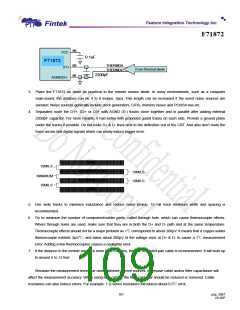
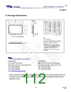
8 PCB Layout Guide
F71872 adopts Current Mode measure method to do temperature detected. The measure data will not be affected by
different process of CPU due to use current mode technology. This technology measures mini-voltage from the remote
sensor so a good PCB layout must be cared about noise minimizing. The noises often come from circuit trace which is a
track from remote sensor (CPU side) to detect circuit input (F71872 side). The signal on this track will be inducted
mini-noises when it passes through a high electromagnetic area. Those effects will result in the mini-noises and show in the
detected side. It will be reported a wrong data which you want to measure. Please pay attention and follow up the check list
below in order to get an actual and real temperature inside the chip.
1. The D1+/D2+/D3+ and AGND (D-) tracks Must Not pass through/by PWM POWER-MOS. Keep as far as possible
from POWER MOS.
2. Place a 0.1µF bypass capacitor close to the VCC pin (Pin# 99). Place an external 2200pF input filter capacitors across
D+, D- and close to the F71872. Near the pin AGND (D-) Must Be placed a through hole into the GND Plane before
connect to the external 2200pF capacitor.
106
July, 2007
V0.28P

 FINTEK [ FEATURE INTEGRATION TECHNOLOGY INC. ]