F71872
1
0
GPIO31_VAL
GPIO30_VAL
R/W
R/W
1
1
0: GPIO31 outputs 0 when in output mode.
1: GPIO31 outputs 1 when in output mode.
0: GPIO30 outputs 0 when in output mode.
1: GPIO30 outputs 1 when in output mode.
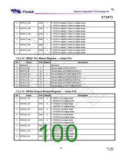
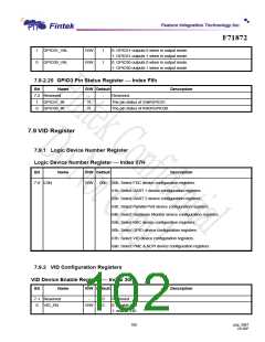
7.8.2.20 GPIO3 Pin Status Register Index F8h
Bit
Name
R/W Default
Description
7-2 Reserved
-
-
-
-
Reserved.
1
0
GPIO31_IN
GPIO30_IN
R
R
The pin status of S3#/GPIO31.
The pin status of IRRX/GPIO30.
7.9 VID Register
7.9.1 Logic Device Number Register
Logic Device Number Register Index 07H
Bit
Name
R/W Default
R/W
Description
7-0 LDN
00h 00h: Select FDC device configuration registers.
01h: Select UART 1 device configuration registers.
02h: Select UART 2 device configuration registers.
03h: Select Parallel Port device configuration registers.
04h: Select Hardware Monitor device configuration registers.
05h: Select KBC device configuration registers.
06h: Select GPIO device configuration registers.
07h: Select VID device configuration registers.
0ah: Select PME & ACPI device configuration registers.
7.9.2 VID Configuration Registers
VID Device Enable Register Index 30h
Bit
Name
R/W Default
Description
7-1 Reserved
VID_EN
-
0
0
Reserved
0
R/W
0: disable VID.
1: enable VID.
100
July, 2007
V0.28P

 FINTEK [ FEATURE INTEGRATION TECHNOLOGY INC. ]