RC4200
PRODUCT SPECIFICATION
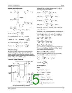
∆VX
----------------
∆VY
200µA
VREF
----------------
R1
=
, R2
=
, Rd = ----------------
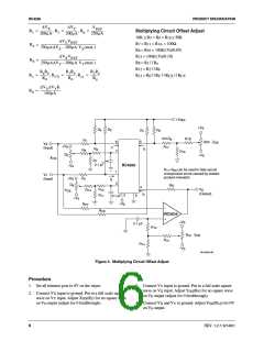
Multiplying Circuit Offset Adjust
10K ≤ R = R = R ≤ 50K
200µA
250µA
5
9
16
∆VXVREF
R = R = R , = 100Ω
7
11 14
Ra = --------------------------------------------------------------------------------
250µA∆VX – 200µA VX(max.)
R = R = 100Ω (V /0.05)
6
10
S
∆VXVREF
250µA∆VY – 200µA VY(max.)
R
= 100Ω (V /0.10)
15
S
Rb = --------------------------------------------------------------------------------
R = R | | R
8
1
a
R
R
= R | | R
2 b
12
13
RaRb
R1Rb
R2Ra
------------
Rd
-------------
Rd
Rc
=
, RCX
=
, Rcy = ------------
Rd
= R | | R | | R | | R
0
C
CX
CY
∆VX∆VYK
R0 = ----------------------------
160µA
+V
REF
+V
S
R
R
a
b
I
R
R
5
d
c
I
100 R
R19
d
R
1
8
7
R20
Z
OS
V
X
+V
R
S
17
(Input)
1
R
4
8
R
6
R
18
R
5
–V
S
X
OS
R
7
0.1 µF
RC4200
–V
S
R
–R can be used to help cancel
17 20
1
2
crossproduct errors caused by resistor
product mismatch.
V
Y
R
+V
2
(Input)
S
I
2
R
9
R
O
4
R
R
V
O
R
12
11
Y
10
OS
(Output)
I
3
3
6
0.1 µF
–V
–V
S
R
S
CY
–
R
CX
RC5534
+
+V
S
0.1 µF
R
13
R
V
OS
16
R
15
R
14
–V
S
65-4200-06
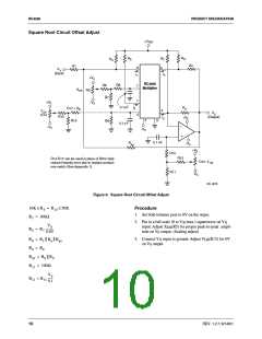
Figure 5. Multiplying Circuit Offset Adjust
Procedure
1. Set all trimmer pots to 0V on the wiper.
3. Connect V input to ground. Put in a full scale square
Y
wave on V input. Adjust Y (R ) for no square wave
OS
X
9
2. Connect V input to ground. Put in a full scale square
X
on V output (adjust for 0 feedthrough).
0
wave on V input. Adjust X (R ) for no square wave
OS
Y
5
on V output (adjust for 0 feedthrough).
4. Connect V and V to ground. Adjust V (R ) for 0V
X Y OS 16
0
on V output.
0
6
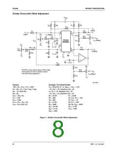
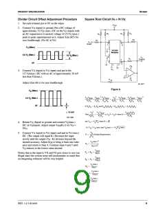
REV. 1.2.1 6/14/01

 FAIRCHILD [ FAIRCHILD SEMICONDUCTOR ]