RC4200
PRODUCT SPECIFICATION
Previous multiplier designs have suffered from an additional
undesired linear term in the above equation; the collector
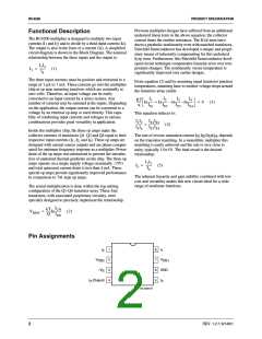
Functional Description
The RC4200 multiplier is designed to multiply two input
current times the emitter resistance. The I r term intro-
C E
currents (I and I ) and to divide by a third input current (I ).
1
2
4
duces a parabolic nonlinearity even with matched transistors.
Fairchild Semiconductor has developed a unique and propri-
etary means of inherently compensating for this undesired
The output is also in the form of a current (I ). A simplified
circuit diagram is shown in the Block Diagram. The nominal
relationship between the three inputs and the output is:
3
I r term. Furthermore, this Fairchild Semiconductor devel-
C E
oped circuit technique compensates linearity error over tem-
perature changes. The nonlinearity versus temperature is
significantly improved over earlier designs.
I1I2
---------
I3
=
(1)
I4
The three input currents must be positive and restricted to a
range of 1 µA to 1 mA. These currents go into the multiplier
chip at op amp summing junctions which are nominally at
zero volts. Therefore, an input voltage can be easily
From equation (2) and by assuming equal transistor junction
temperatures, summing base-to-emitter voltage drops around
the transistor array yields:
I1
I2
I3
I4
converted to an input current by a series resistor. Any
number of currents may be summed at the inputs. Depending
on the application, the output current can be converted to a
voltage by an external op amp or used directly. This capa-
bilty of combining input currents and voltages in various
combinations provides great versatility in application.
KT
-------
q
-------
IS1
-------
IS2
-------
IS3
-------
IS4
In
= In
– In
–In
= 0 (3)
This equation reduces to:
IS1 S2
I
I1I2
---------------
--------- =
I3I4
(4)
IS3 S4
I
Inside the multiplier chip, the three op amps make the
collector currents of transistors Q1, Q2 and Q4 equal to their
respective input currents (I , I , and I ). These op amps are
The rate of reverse saturation current I I /I I , depends
S1 S2 S3 S4
on the transistor matching. In a monolithic multiplier this
matching is easily achieved and the rate is very close to
unity, typically 1.0 1%. The final result is the desired
relationship:
1
2
4
designed with current source outputs and are phase-compen-
sated for optimum frequency response as a multiplier. Power
drain of the op amps was minimized to prevent the introduc-
tion of undesired thermal gradients on the chip. The three op
amps operate on a single supply voltage (nominally -15V)
and total quiescent current drain is less than 4 mA. These
special op amps provide significantly improved performance
in comparison to 741-type op amps.
I1I2
---------
I3
=
(5)
I4
The inherent linearity and gain stability combined with low
cost and versatility makes this new circuit ideal for a wide
range of nonlinear functions.
The actual multiplication is done within the log-antilog
configuration of the Q1-Q4 transistor array. These four
transistors, with associated proprietary circuitry, were
specially designed to precisely implement the relationship.
ICN
kT
------ --------
VBEN
=
In
(2)
Q
ISN
Pin Assignments
I
1
2
3
4
8
7
6
5
I
1
2
V
V
OS2
–V
OS1
GND
S
I
(Output)
I
4
3
65-4200-07
2
REV. 1.2.1 6/14/01

 FAIRCHILD [ FAIRCHILD SEMICONDUCTOR ]