PRODUCT SPECIFICATION
RC4200
Resistors R and R extend the range of the V and V
Y
inputs by picking values such that:
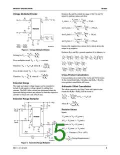
Voltage Multiplier/Divider
a
b
X
R
4
R
1
8
5
VX(min.) VREF
V
Z
V
V
X
Y
I1(min.) = ----------------------- + ------------- = 50 µA,
I
I
1
R1
Ra
4
7
VX(max.) VREF
and I1(max.) = ----------------------- + ------------- = 250 µA,
R1 Ra
RC4200
R
2
1
2
VY(min.) VREF
also I2(min.) = ---------------------- + ------------- = 50 µA,
I
2
R2
Rb
4
V
R
O
O
I
VY(max.) VREF
3
3
S
6
and I2(max.) = ----------------------- + ------------- = 250 µA.
R2
Rb
–V
V V
R R
1
V V
O Z
R R
O 4
X
Y
=
Resistor R supplies bias current for I which allows the
C
3
65-4200-04
2
output to go negative.
Figure 3. Voltage Multiplier/Divider
Resistors R and R permit equation (6) to balance, ie.:
CX
CY
VXVY R0R4
Solving for V0 = -------------------------------------
V
V
V
V
V
V
V
V
V
VZ
R1R2
REF
X
REF
Y
REF
0
REF
X
Y
---------------
-------- + --------------- -------- + ---------------
=
------ + --------------- + ------------ + ------------
R
D
R
R
R
R
R
R
R
R
1
a
2
b
0
C
CX
CY
For a multiplier circuit VZ = VR = constant
V
V
V
V
V
V V
REF
Y
X
X
REF
Y REF
---------------
----------------- + ------------------------- + ------------------------- +
=
R R
R R
1
R R
R R
R0R4
a
b
2
1
b
2 a
Therefore: V0 = VXVYK where K = ---------------------
VRR1R2
2
V
V V
V
V
V V
REF
0
REF
X
REF
Y REF
----------------
----------------------- + ------------------------- + ------------------------- +
R R
R R
R
R
R
R
c
d
0
d
cx
d
CY d
For a divider circuit VY = VR = constant
VX
VRR0R4
Cross-Product Cancellation
Cross-products are a result of ths V V and V V terms.
-------
VZ
Therefore: V0
=
K where K = ---------------------
R1R2
X
R
Y R
To the extend that R R = R R , and R R = R
R
CY d
1 b CX D 2 a
cross-product cancellation will occur.
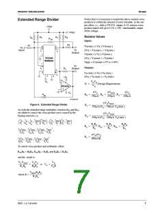
Extended Range
The input and output voltage ranges can be extended to
include 0 and negative voltage signals by adding bias
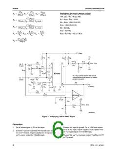
Arithmetic Offset Cancellation
The offset caused by the V
REF
2 term will cancel to the
currents. The R C filter circuits are eliminated when the
S S
extent that R R = R R , and the result is:
a b
0 d
input and biasing resistors are selected to limit the respective
currents to 50 µA min. and 250 µA max.
V0VREF
VYVX
--------------------
R0Rd
--------------- =
R1R2
or V0 = VXVYK
Extended Range Multiplier
R0Rd
+VREF
---------------------------
where K =
VREFR1R2
R
R
R
5
R
D
A
B
C
I
8
V
X
Resistor Values
(Input)
R
1
I
1
4
Inputs:
7
VX(min.) ≤ VX ≤ VX(max.)
∆VX = VX(max.) – VX(min.)
VY(min.) ≤ VY ≤ VY(max.)
∆VY = VY(max.) = VY(min.)
VREF = Constant (+7V to +18V)
V0
RC4200
R
2
1
2
V
Y
V
O
(Input)
I
2
R
O
(Output)
4
I
3
3
6
S
+V
S
R
–V
C4
R
–V
S
CX
---------------
K =
(Design Requirements)
VXVY
65-4200-05
Figure 4. Extended Range Multiplier
REV. 1.2.1 6/14/01
5

 FAIRCHILD [ FAIRCHILD SEMICONDUCTOR ]