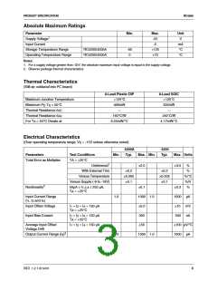
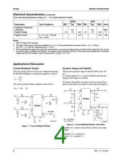
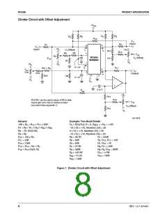
PRODUCT SPECIFICATION
RC4200
Notice that it is necessary to match the above resistor cross-
products to within the amount of error tolerable in the out-
put offset, i.e., with a 10V F.S. output, 0.1% resistor cross-
product match will give 0.1% x 10V. untrimmable output
offset voltage.
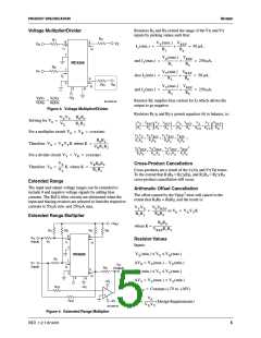
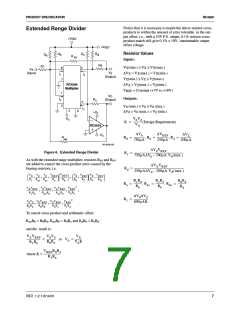
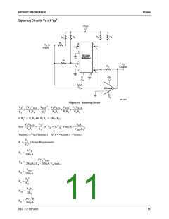
Extended Range Divider
+V
REF
+V
REF
Resistor Values
Inputs:
R
R
R
5
R
d
b
c
a
R
az
R4
R1
V (min.) ≤ V ≤ V (max.)
8
X
X
X
V
X
V
(Input)
Z
∆V = V (max.) = V (min.)
X
X
X
I1
I4
(Output)
V (min.) ≤ V ≤ V (max.)
Z
Z
Z
7
1
RC4200
Multiplier
∆V = V (max.) = V (min.)
Z
Z
Z
V
REF
= Constant (+7V to +18V)
V
O
Outputs:
V (min.) ≤ V ≤ V (max.)
I2
RO
(Output)
4
2
0
0
0
I3
3
6
∆V = V (max.) = V (min.)
0
0
0
+VS
-VS
V0VZ
--------------
VX
K =
(Design Requirement)
RC5534
∆V0
750µA
∆VREF
250µA
∆VZ
200µA
-VS
R
----------------
-----------------
= , R4 = ----------------
R0
=
, Rb
ao
65-4200-08
∆V0VREF
750µA∆V0 – 700µA V0(max.)
Figure 6. Extended Range Divider
Rc = ------------------------------------------------------------------------------
As with the extended range multiplier, resistors R and R
az
ao
are added to cancel the cross-product error caused by the
biasing resistors, i.e.
∆VXVREF
250µA∆VZ – 200µA VZ(max.)
Rd = -------------------------------------------------------------------------------
V
---------------
V
V
V
V
V
V
V
V
REF
R
b
X
0
Z
REF
0
REF
Z
REF
-------- + --------- + --------- + ---------------
=
------ + --------------- ------- + ---------------
R
R
R
R
R
R
R
R
1
ao
az
a
0
C
4
D
RcRd
RcR4
R0Rd
------------
Rb
------------
Rb
Ra
=
, Raz
=
, Rao = -------------
Rb
2
V
V
V
V V
V
V
REF
X
REF
0
REF
Z
REF
R
----------------
------------------------- + ----------------------- + ------------------------ +
=
R R
R R
R
R
R
a
b
1
b
ao
b
az b
∆V0∆VZ
R1 = ----------------------
600µAK
2
V
V V
V V
V V
REF
0
Z
0
REF
Z
REF
----------------
--------------- + ----------------------- + ------------------------ +
R R
R R
R R
R R
c
d
0
4
0
d
4 c
To cancel cross-product and arithmetic offset:
R
R = R R , R R = R R and R R = R R
ao b 0 d az b 4 c a b c d
and the result is:
V0VZ
--------------
VX
-----------
or V0 =
VXVREF
--------------------- =
R1Rb
R0R4
VZK
V
REFR0R4
---------------------------
where K =
R1Rb
REV. 1.2.1 6/14/01
7

 FAIRCHILD [ FAIRCHILD SEMICONDUCTOR ]