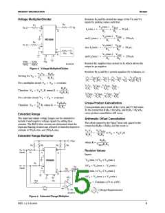
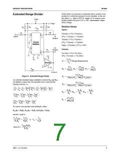
PRODUCT SPECIFICATION
RC4200
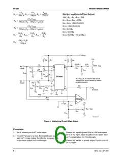
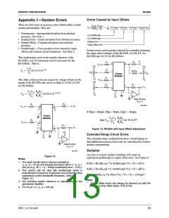
Divider Circuit Offset Adjustment Procedure
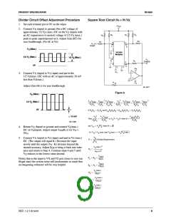
Square Root Circuit V = N√V
0
X
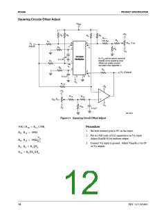
1. Set each trimmer pot to 0V on the wiper.
+VREF
2. Connect V (input) to ground. Put a DC voltage of
X
approximatey 1/2 V (max.) DC on the V (input) with
Z
Z
R
R
R
5
R
d
b
c
an AC (squarewave is easiest) voltage of 1/2 V (max.)
a
Z
peak-to-peak superimposed on it. Adjust X (R5) for
OS
zero feedthrough. (No AC at V )
0
R4
R1
8
VX
(Input)
I
I
1
4
V
(Max.)
7
z
RC4200
Multiplier
1/2 V (Max.)
z
1
2
1/2 V (Max.)
z
VO
(Output)
I
RO
2
4
I
0V
3
3
6
+VS
-VS
3. Connect V (input) to V (input) and put in the
X
Z
1/2 V (max.) DC with an AC of approximately 20 mV
Z
less than V (max.).
Z
R
-VS
ao
Adjust Z (R ) for zero feedthrough.
OS 13
65-1877
Figure 8.
V
(Max.)
z
2
2
2
V
V
V
V V
V
V V
V V
V
1/2 V (Max.)
z
X
REF
REF
0
REF
0
0
REF
0
REF
REF
------------------------- + ---------------- + ----------------------- = -------------- + ----------------------- + ----------------------- + ----------------
R R
R R
R
R
R R
R R
R
R
R R
1
b
a
b
ao
b
0
4
c
4
d
c d
0
0V
If R R = R R and R R R R + R R R R = R R R R
a
b
c
d
ao
b
0
d
ao
b
c
4
c
d 0 4
2
~
10 mV
V
V
V
V
R R
~
0
X
REF
REF 0 4
2
--------------
-------------------------
-------------------------------
Then
=
or V = V K where K =
0
X
R R
R R
R R
0
4
1
b
1 b
65-1868
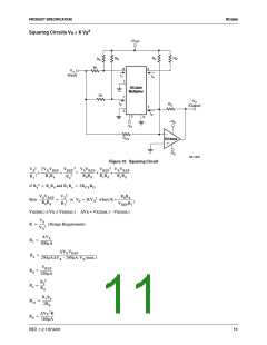
and V = N
V
where N =
K
0
X
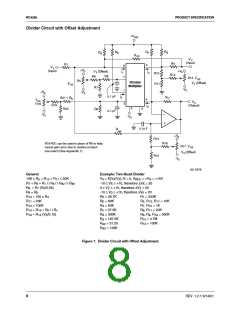
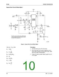
4. Return V (Input) to ground and connect V (max.)
X
Z
DC on V (input). Adjust output V (R ) for V
=
O
Z
OS 17
0 ≤ V ≤ V (max.)and V (max.) = N
V (max.)
X
X
X
0
0V
O
V
------------
V
X
5. Connect V (input) to V (input) and and in V (max.)
X
Z
Z
0
N =
(Design Requirements)
DC. (The output will equal K.) Decrease the input
slowly until the output (V - K) deviates beyond the
0
desired accuracy. Adjust Z to bring it back into toler-
OS
ance and return to Step 4. Continue steps 4 and 5 until
2
V (max.)
0
R
1
= ---------------------------
2
74µA N
V reduces to the lowest value desired.
Z
V
REF
R
R
= R = ---------------
a
d
Notice that as the input to VX and VZ gets closer to zero (an
illegal state) the system noise will predominate so much that
an integrating voltmeter will be very helpful.
50µA
V
REF
= R = -----------------
b
c
150µA
V (max.)
0
50µA
R
= ------------------------
4
V (max.)
0
125µA
R
R
= ------------------------
ao
0
V (max.)
0
= ------------------------
225µA
REV. 1.2.1 6/14/01
9

 FAIRCHILD [ FAIRCHILD SEMICONDUCTOR ]