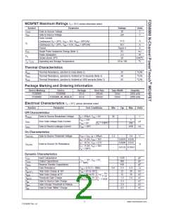
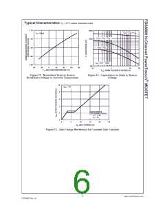
Switching Characteristics (VGS = 10V)
tON
td(ON)
tr
Turn-On Time
Turn-On Delay Time
Rise Time
-
-
-
-
-
-
-
51
-
ns
ns
ns
ns
ns
ns
7
27
38
15
-
-
VDD = 15V, ID = 11.6A
GS = 10V, RGS = 11Ω
V
td(OFF)
tf
Turn-Off Delay Time
Fall Time
-
-
tOFF
Turn-Off Time
80
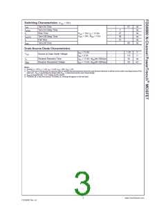
Drain-Source Diode Characteristics
I
SD = 11.6A
-
-
-
-
-
-
-
-
1.25
1.0
30
V
V
VSD
Source to Drain Diode Voltage
ISD = 2.1A
trr
Reverse Recovery Time
ISD = 11.6A, dISD/dt=100A/µs
ISD = 11.6A, dISD/dt=100A/µs
ns
nC
QRR
Reverse Recovered Charge
20
Notes:
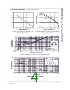
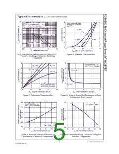
1: Starting T = 25°C, L = 1mH, I = 12.8A, V = 30V, V = 10V.
J
AS
DD
GS
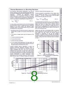
2: R
is the sum of the junction-to-case and case-to-ambient thermal resistance where the case thermal reference is defined as the solder mounting surface of the
θJA
drain pins. R
is guaranteed by design while R
is determined by the user’s board design.
θJC
θJA
2
3: R
is measured with 1.0 in copper on FR-4 board
θJA
4: FDS8880_NL is lead free product. FDS8880_NL marking will appear on the reel label.
3
www.fairchildsemi.com
FDS8880 Rev. A1

 FAIRCHILD [ FAIRCHILD SEMICONDUCTOR ]