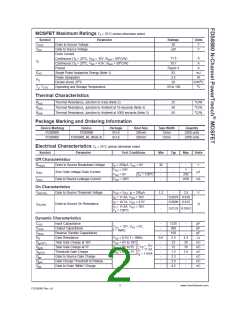
MOSFET Maximum Ratings TA = 25°C unless otherwise noted
Symbol
VDSS
VGS
Parameter
Ratings
30
Units
Drain to Source Voltage
Gate to Source Voltage
Drain Current
V
V
±20
Continuous (TA = 25oC, VGS = 10V, RθJA = 50oC/W)
Continuous (TA = 25oC, VGS = 4.5V, RθJA = 50oC/W)
Pulsed
11.6
10.7
A
A
ID
Figure 4
82
A
EAS
Single Pulse Avalanche Energy (Note 1)
mJ
Power dissipation
Derate above 25oC
2.5
W
PD
20
mW/oC
oC
TJ, TSTG
Operating and Storage Temperature
-55 to 150
Thermal Characteristics
RθJC
RθJA
RθJA
Thermal Resistance, Junction to Case (Note 2)
25
50
85
oC/W
oC/W
oC/W
Thermal Resistance, Junction to Ambient at 10 seconds (Note 3)
Thermal Resistance, Junction to Ambient at 1000 seconds (Note 3)
Package Marking and Ordering Information
Device Marking
FDS8880
Device
FDS8880
Package
SO-8
Reel Size
330mm
Tape Width
Quantity
12mm
12mm
2500 units
2500 units
FDS8880
FDS8880_NL (Note 4)
SO-8
330mm
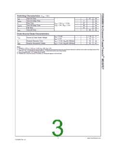
Electrical Characteristics TA = 25°C unless otherwise noted
Symbol
Parameter
Test Conditions
Min
Typ
Max
Units
Off Characteristics
BVDSS
Drain to Source Breakdown Voltage
Zero Gate Voltage Drain Current
Gate to Source Leakage Current
ID = 250µA, VGS = 0V
30
-
-
-
-
-
-
V
V
DS = 24V
1
IDSS
µA
VGS = 0V
TA = 150oC
-
250
±100
IGSS
VGS = ±20V
-
nA
On Characteristics
VGS(TH)
Gate to Source Threshold Voltage
VGS = VDS, ID = 250µA
1.2
-
2.5
V
ID = 11.6A, VGS = 10V
-
-
0.0079 0.010
0.0096 0.012
I
D = 10.7A, VGS = 4.5V
rDS(ON)
Drain to Source On Resistance
Ω
ID = 11.6A, VGS = 10V,
TA = 150oC
-
0.0125 0.0163
Dynamic Characteristics
CISS
COSS
CRSS
RG
Input Capacitance
-
1235
260
150
2.5
23
-
-
pF
pF
pF
Ω
VDS = 15V, VGS = 0V,
f = 1MHz
Output Capacitance
-
Reverse Transfer Capacitance
Gate Resistance
-
-
VGS = 0.5V, f = 1MHz
VGS = 0V to 10V
0.6
4.3
30
16
1.6
-
Qg(TOT)
Qg(5)
Qg(TH)
Qgs
Total Gate Charge at 10V
Total Gate Charge at 5V
Threshold Gate Charge
Gate to Source Gate Charge
Gate Charge Threshold to Plateau
Gate to Drain “Miller” Charge
-
-
-
-
-
-
nC
nC
nC
nC
nC
nC
VDD = 15V
D = 11.6A
Ig = 1.0mA
VGS = 0V to 5V
VGS = 0V to 1V
12
I
1.3
3.3
2.0
4.2
Qgs2
Qgd
-
-
2
www.fairchildsemi.com
FDS8880 Rev. A1

 FAIRCHILD [ FAIRCHILD SEMICONDUCTOR ]