FAN5066
PRODUCT SPECIFICATION
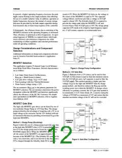
Input Filter
PCB Layout Guidelines
The DC-DC converter design may include an input inductor
between the system +5V supply and the converter input as
shown in Figure 6. This inductor serves to isolate the +5V
supply from the noise in the switching portion of the DC-DC
converter, and to limit the inrush current into the input capac-
itors during power up. A value of 2.5µH is recommended.
• Placement of the MOSFETs relative to the FAN5066 is
critical. Place the MOSFETs such that the trace length of
the HIDRV and LODRV pins of the FAN5066 to the FET
gates is minimized. A long lead length on these pins will
cause high amounts of ringing due to the inductance of the
trace and the gate capacitance of the FET. This noise
radiates throughout the board, and, because it is switching
at such a high voltage and frequency, it is very difficult to
suppress.
• In general, all of the noisy switching lines should be kept
away from the quiet analog section of the FAN5066. That
is, traces that connect to pins 9, 12, and 13 (LODRV,
HIDRV and VCCQP) should be kept far away from the
traces that connect to pins 1 through 5, and pin 16.
• Place the 0.1µF decoupling capacitors as close to the
FAN5066 pins as possible. Extra lead length on these
reduces their ability to suppress noise.
It is necessary to have some low ESR aluminum electrolytic
capacitors at the input to the converter. These capacitors
deliver current when the high side MOSFET switches on.
Figure 7 shows 3 x 1000µF, but the exact number required
will vary with the speed and type of the processor. For the
top speed Klamath and Deschutes, the capacitors should be
rated to take 7A of ripple current. Capacitor ripple current
rating is a function of temperature, and so the manufacturer
should be contacted to find out the ripple current rating at the
expected operational temperature. For details on the design
of an input filter, refer to Applications Bulletin AB-15.
• Each VCC and GND pin should have its own via to the
appropriate plane. This helps provide isolation between
pins.
2.5µH
5V
Vin
• Surround the CEXT timing capacitor with a ground trace.
Be sure to place a ground or power plane underneath the
capacitor for further noise isolation, in order to provide
additional shielding to the oscillator (pin 1) from the noise
on the PCB. In addition, place this capacitor as close to
pin 1 as possible.
1000µF, 10V
Electrolytic
0.1µF
• Place the MOSFETs, inductor, and Schottky as close
together as possible for the same reasons as in the first
bullet above. Place the input bulk capacitors as close to
the drains of the high side MOSFETs as possible. In
addition, placement of a 0.1µF decoupling cap right on
the drain of each high side MOSFET helps to suppress
some of the high frequency switching noise on the input
of the DC-DC converter.
Figure 7. Input Filter
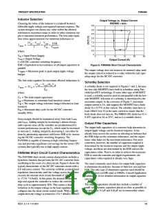
Droop Resistor
Figure 8 shows a converter using a “droop resistor”, R . The
D
function of the droop resistor is to improve the transient
response of the converter, potentially reducing the number of
output capacitors required. In operation, the droop resistor
causes the output voltage to be slightly lower at heavy load
current than it otherwise would be. When the load transitions
from heavy to light current, the output can swing up farther
without exceeding limits, because it started from a lower
voltage, thus reducing the capacitor requirements.
• Place the output bulk capacitors as close to the CPU as
possible to optimize their ability to supply instantaneous
current to the load in the event of a current transient.
Additional space between the output capacitors and the
CPU will allow the parasitic resistance of the board traces
to degrade the DC-DC converter’s performance under
severe load transient conditions, causing higher voltage
deviation. For more detailed information regarding
capacitor placement, refer to Application Bulletin AB-5.
• The traces that run from the FAN5066 IFB (pin 4) and
VFB (pin 5) pins should be run together next to each other
and Kelvin connected to the sense resistor. Running these
lines together rejects some of the common mode noise
that is presented to the FAN5066 feedback input. Try, as
much as possible, to run the noisy switching signals
(HIDRV, LODRV & VCCQP) on one layer, but use the
inner layers for power and ground only. If the top layer is
being used to route all of the noisy switching signals, use
the bottom layer to route the analog sensing sign VFB and
IFB.
Q1
RSENSE
RDROOP
L2
VO
COUT
Q2
IFB
VFB
Figure 8. Use of a Droop Resistor
• A PC Board Layout Checklist is available from Fairchild
Applications. Ask for Application Bulletin AB-11.
14
REV. 2.1.4 11/13/01

 FAIRCHILD [ FAIRCHILD SEMICONDUCTOR ]