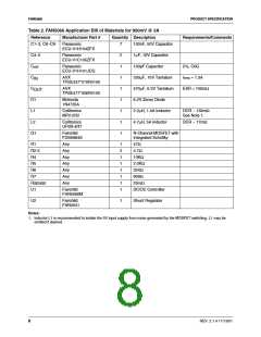
FAN5066
PRODUCT SPECIFICATION
In general, a higher operating frequency decreases the peak
ripple current flowing in the output inductor, thus allowing
the use of a smaller inductor value. In addition, operation at
higher frequencies decreases the amount of energy storage
that must be provided by the bulk output capacitors during
load transients due to faster loop response of the controller.
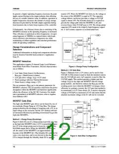
mately 4.5V. When the MOSFET Q1 turns on, the voltage at
the source of the MOSFET is equal to 5V. The capacitor
voltage follows, and hence provides a voltage at VCCQP
equal to almost 10V. The Schottky diode D1 is required to
provide the charge path when the MOSFET is off, and
reverses biases when VCCQP goes to 10V. The charge pump
capacitor (CP) needs to be a high Q, high frequency capaci-
tor. A 1µF ceramic capacitor is recommended here.
Unfortunately, the efficiency losses due to switching of the
MOSFETs increase as the operating frequency is increased.
Thus, efficiency is optimized at lower frequencies. An oper-
ating frequency of 300KHz is a typical choice which opti-
mizes efficiency and minimizes component size while
maintaining excellent regulation and transient performance
under all operating conditions.
+5V
D1
VCCQP
HIDRV
Q1
CP
Design Considerations and Component
Selection
L2 RS
VO
PWM/PFM
Control
Additional information on design and component selection
may be found in Fairchild Semiconductor’s Application
Note 53.
COUT
LODRV
GNDP
Q2
D2
MOSFET Selection
This application requires N-channel Logic Level Enhance-
ment Mode Field Effect Transistors. Desired characteristics
are as follows:
Figure 4. Charge Pump Configuration
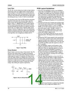
Method 2. 12V Gate Bias
Figure 5 illustrates how a 12V source can be used to bias
VCCQP. A 47Ω resistor is used to limit the transient current
into the VCCQP pin and a 1µF capacitor is used to filter the
VCCQP supply. This method provides a higher gate bias
• Low Static Drain-Source On-Resistance,
R
< 20mΩ (lower is better)
DS,ON
• Low gate drive voltage, V = 4.5V rated
GS
• Power package with low Thermal Resistance
• Drain-Source voltage rating > 15V.
voltage (V ) to the high side MOSFET than the charge
GS
pump method, and therefore reduces the R
and the
DS,ON
The on-resistance (R ) is the primary parameter for
DS,ON
resulting power loss within the MOSFET. In designs where
efficiency is a primary concern, the 12V gate bias method is
recommended. A 6.2V Zener diode, D1, is used to clamp the
voltage at VCCQP to a maximum of 12V and ensure that the
absolute maximum voltage of the IC will not be exceeded.
MOSFET selection. The on-resistance determines the power
dissipation within the MOSFET and therefore significantly
affects the efficiency of the DC-DC Converter. For details
and a spreadsheet on MOSFET selection, refer to Applica-
tions Bulletin AB-8
+5V
MOSFET Gate Bias
+12V
47Ω
D1
The high side MOSFET gate driver can be biased by one of
two methods–Charge Pump or 12V Gate Bias. The charge
pump method has the advantage of requiring only +5V as an
input voltage to the converter, but the 12V method will real-
ize increased efficiency by providing an increased V to the
GS
high side MOSFETs.
VCCQP
Q1
HIDRV
1µF
L2 RS
VO
PWM/PFM
Control
Method 1. Charge Pump (Bootstrap)
COUT
Figure 4 shows the use of a charge pump to provide gate bias
to the high side MOSFET when +12V is unavailable. Capac-
itor CP is the charge pump used to boost the voltage of the
FAN5066 output driver. When the MOSFET Q1 switches
off, the source of the MOSFET is at approximately 0V
because of the MOSFET Q2. (The Schottky D2 conducts for
only a very short time, and is not relevent to this discussion.)
CP is charged through the Schottky diode D1 to approxi-
LODRV
Q2
D2
GNDP
Figure 5. Gate Bias Configuration
12
REV. 2.1.4 11/13/01

 FAIRCHILD [ FAIRCHILD SEMICONDUCTOR ]