ST16C650A
2.90V TO 5.5V UART WITH 32-BYTE FIFO
áç
REV. 5.0.0
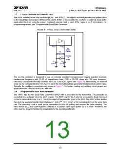
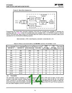
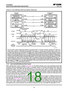
FIGURE 8. BAUD RATE GENERATOR
DLL and DLM
Registers
M CR Bit-7=0
(default)
Prescaler
Divide by 1
16X
Crystal
O sc/
Buffer
XTAL1
XTAL2
Sam pling
Rate Clock to
Transm itter
Baud Rate
G enerator
Logic
Prescaler
Divide by 4
M CR Bit-7=1
Programming the Baud Rate Generator Registers DLM and DLL provides the capability of selecting the
operating data rate. Table 4 shows the standard data rates available with a 14.7456 MHz crystal or external
clock at 16X clock rate. When using a non-standard data rate crystal or external clock, the divisor value can be
calculated for DLL/DLM with the following equation.
divisor (decimal) = (XTAL1 clock frequency / prescaler) / (serial data rate x 16)
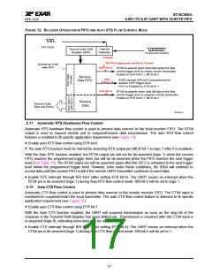
TABLE 4: TYPICAL DATA RATES WITH A 14.7456 MHZ CRYSTAL OR EXTERNAL CLOCK
DLM
PROGRAM
VALUE (HEX) VALUE (HEX)
DLL
PROGRAM
DATA RATE
ERROR (%)
OUTPUT Data Rate OUTPUT Data Rate DIVISOR FOR 16x DIVISOR FOR 16x
MCR Bit-7=1
MCR Bit-7=0
Clock (Decimal) Clock (HEX)
100
600
400
2304
384
192
96
48
24
12
6
900
180
C0
60
09
01
00
00
00
00
00
00
00
00
00
00
80
C0
60
30
18
0C
06
04
02
01
0
0
0
0
0
0
0
0
0
0
0
2400
1200
2400
4800
9600
19.2k
38.4k
57.6k
115.2k
230.4k
4800
9600
19.2k
38.4k
76.8k
153.6k
230.4k
460.8k
921.6k
30
18
0C
06
4
04
2
02
1
01
2.9
Transmitter
The transmitter section comprises of an 8-bit Transmit Shift Register (TSR) and 32 bytes of FIFO which
includes a byte-wide Transmit Holding Register (THR). TSR shifts out every data bit with the 16X internal
clock. A bit time is 16 clock periods. The transmitter sends the start-bit followed by the number of data bits,
inserts the proper parity-bit if enabled, and adds the stop-bit(s). The status of the FIFO and TSR are reported in
the Line Status Register (LSR bit-5 and bit-6).
14

 EXAR [ EXAR CORPORATION ]