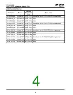
ST16C1550/51
2.97V TO 5.5V UART WITH 16-BYTE FIFO
áç
REV. 4.2.0
2.0 FUNCTIONAL DESCRIPTIONS
2.1
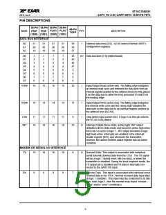
Internal Registers
The 155X has a set of enhanced registers for controlling, monitoring and data loading and unloading. These
registers function as data holding registers (THR/RHR), interrupt status and control registers (ISR/IER), a FIFO
control register (FCR), receive line status and control registers (LSR/LCR), modem status and control registers
(MSR/MCR), programmable data rate (clock) divisor registers (DLL/DLM), and a user accessible scractchpad
register (SPR). All the register functions are discussed in full detail later in “Section 3.0, UART INTERNAL
REGISTERS” on page 14.
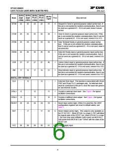
2.2
DMA Mode
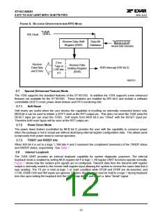
The DMA Mode (a legacy term) in this document does not mean “Direct Memory Access” but refers to data
block transfer operation. The DMA mode affects the state of the RXRDY and TXRDY bits (ISR bits 5 and 4
respectively). The transmit and receive FIFO trigger levels provide additional flexibility to the user for block
mode operation. The LSR bits 5-6 provide an indication when the transmitter is empty or has an empty
location(s) for more data. The user can optionally operate the transmit and receive FIFO in the DMA mode
(FCR bit-3=1). When the transmit and receive FIFO are enabled and the DMA mode is disabled (FCR bit-3 =
0), the 155X activates the TXRDY & RXRDY output pin for each data transmit or receive operation. When
DMA mode is enabled (FCR bit-3 = 1), the user takes advantage of block mode operation by loading or
unloading the FIFO in a block sequence determined by the programmed trigger level. In this mode, the 155X
sets the TXRDY bit when the transmit FIFO becomes full, and sets the RXRDY pin when the receive FIFO
becomes empty. The following table shows their behavior.
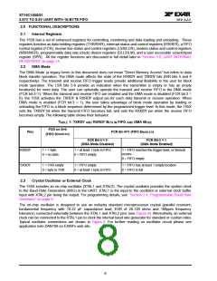
TABLE 1: TXRDY AND RXRDY BITS IN FIFO AND DMA MODE
FCR BIT-0=0
PINS
FCR BIT-0=1 (FIFO ENABLED)
(FIFO DISABLED)
FCR Bit-3 = 0
FCR Bit-3 = 1
(DMA Mode Disabled)
(DMA Mode Enabled)
RXRDY
1 = 1 byte
1 = at least 1 byte in FIFO
0 = FIFO empty
1 = FIFO reaches the trigger level, or timeout
occurs
0 = no data
0 = FIFO empty
TXRDY
1 = THR empty
0 = byte in THR
1 = FIFO empty
1 = FIFO has at least 1 empty location
0 = FIFO is full
0 = at least 1 byte in FIFO
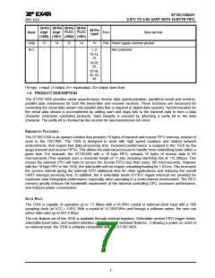
2.3
Crystal Oscillator or External Clock
The 155X includes an on-chip oscillator (XTAL1 and XTAL2). The crystal oscillator provides the system clock
to the Baud Rate Generators (BRG) in the UART. XTAL1 is the input to the oscillator or external clock buffer
input with XTAL2 pin being the output. For programming details, see “Section 2.4, Programmable Baud Rate
Generator” on page 9.
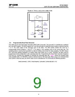
The on-chip oscillator is designed to use an industry standard microprocessor crystal (parallel resonant,
fundamental frequency with 10-22 pF capacitance load, ESR of 20-120 ohms and 100ppm frequency
tolerance) connected externally between the XTAL1 and XTAL2 pins (see Figure 4). Alternatively, an external
clock can be connected to the XTAL1 pin to clock the internal baud rate generator for standard or custom rates.
Typical oscillator connections are shown in Figure 4. For further reading on oscillator circuit please see
application note DAN108 on EXAR’s web site.
8

 EXAR [ EXAR CORPORATION ]