áç
ST16C1550/51
2.97V TO 5.5V UART WITH 16-BYTE FIFO
REV. 4.2.0
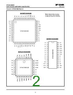
PIN DESCRIPTIONS
28-PIN 28-PIN 28-PIN 28-PIN
PLCC PLCC
(1550) (1551) (1550) (1551)
48-PIN
TQFP
NAME
TYPE
DESCRIPTION
PDIP
PDIP
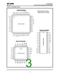
DATA BUS INTERFACE
A0
A1
A2
21
20
19
21
20
19
21
20
19
21
20
19
30
28
27
I
Address data lines [2:0]. A2:A0 selects internal UART’s
configuration registers.
D0
D1
D2
D3
D4
D5
D6
D7
1
2
3
4
5
6
7
8
1
2
3
4
5
6
7
8
1
2
3
4
5
6
7
8
1
2
3
4
5
6
7
8
43
45
46
47
3
I/O Data bus lines [7:0] (bidirectional).
4
5
6
IOR#
16
15
16
15
20
17
I
I
Input/Output Read (active low). The falling edge instigates
an internal read cycle and retrieves the data byte from an
internal register pointed by the address lines [A2:A0], places
it on the data bus to allow the host processor to read it on
the leading edge.
IOW#
14
13
14
13
Input/Output Write (active low). The falling edge instigates
the internal write cycle and the rising edge transfers the
data byte on the data bus to an internal register pointed by
the address lines [A2:A0].
CS#
INT
11
18
11
18
11
18
11
18
9
I
Chip Select input (active low). A logic 0 on this pin selects
the ST16C155X device.
23
O
Interrupt Output (three-state, active high). INT output
defaults to three-state mode and becomes active high when
MCR bit-3 is set to a logic 1. INT output becomes a logic
high level when interrupts are enabled in the interrupt
enable register (IER), and whenever the transmitter,
receiver, line and/or modem status register has an active
condition.
MODEM OR SERIAL I/O INTERFACE
TX
10
10
10
10
8
7
O
Transmit Data. This output is associated with individual
serial transmit channel data from the 155X. The TX signal
will be a logic 1 during reset, idle (no data), or when the
transmitter is disabled. During the local loopback mode, the
TX output pin is disabled and TX data is internally con-
nected to the UART RX input.
RX
9
9
9
9
I
Receive Data. This input is associated with individual serial
channel data to the 155X. Normal received data input idles
at logic 1 condition. This input must be connected to its idle
logic state, logic 1, else the receiver may report “receive
break” and/or “error” condition(s).
5

 EXAR [ EXAR CORPORATION ]