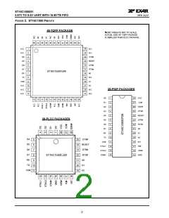
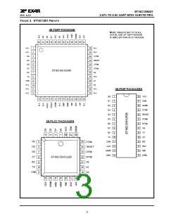
ST16C1550/51
2.97V TO 5.5V UART WITH 16-BYTE FIFO
áç
REV. 4.2.0
28-PIN 28-PIN 28-PIN 28-PIN
48-PIN
TQFP
PLCC PLCC
NAME
TYPE
DESCRIPTION
PDIP
PDIP
(1550) (1551) (1550) (1551)
RTS#
22
22
22
22
31
O
Request to Send or general purpose output (active low). If
this pin is not needed for modem communication, then it can
be used as a general I/O. If it is not used, leave it uncon-
nected.
CTS#
DTR#
25
23
25
23
25
23
25
23
34
32
I
Clear to Send or general purpose input (active low). If this
pin is not needed for modem communication, then it can be
used as a general I/O. If it is not used, connect it to VCC.
O
Data Terminal Ready or general purpose output (active
low). If this pin is not needed for modem communication,
then it can be used as a general I/O. If it is not used, leave it
unconnected.
DSR#
26
26
26
26
39
I
Data Set Ready input or general purpose input (active low).
If this pin is not needed for modem communication, then it
can be used as a general I/O. If it is not used, connect it to
VCC.
CD#
RI#
27
17
27
16
27
17
27
16
40
21
I
I
Carrier Detect input or general purpose input (active low). If
this pin is not needed for modem communication, then it can
be used as a general I/O. If it is not used, connect it to VCC.
Ring Indicator input or general purpose input (active low). If
this pin is not needed for modem communication, then it can
be used as a general I/O. If it is not used, connect it to VCC.
ANCILLARY SIGNALS
CLK
-
12
-
12
-
I
External Clock Input. This function is associated with 28 pin
PDIP and 28 pin PLCC packages only. An external clock
must be connected to this pin to clock the baud rate genera-
tor and internal circuitry.
XTAL1
XTAL2
RESET
12
13
24
-
-
12
13
24
-
-
15
16
33
I
O
I
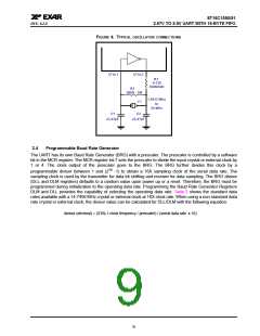
Crystal or external clock input. See Figure 4 for typical
oscillator connections.
Crystal or buffered clock output. See Figure 4 for typical
oscillator connections.
24
24
Reset Input (active high). When it is asserted, the UART
configuration registers are reset to default values, see
Table 8.
RST
-
17
28
-
17
28
22
O
Reset Output (active high). This output is only available on
the ST16C1551. When IER bit-5 is a logic 0, RST will follow
the logical state of the RESET pin. When IER bit-5 is a logic
1, the user may send software (soft) resets via MCR bit-2.
Soft resets from MCR bit-2 are “ORed” with the state of the
RESET pin.
VCC
28
28
41
Pwr Power supply input.
6

 EXAR [ EXAR CORPORATION ]