EMD3D256M08BS1
EMD3D256M16BS1
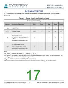
DC CHARACTERISTICS
DC Characteristics are defined under standard measurement conditions specified in JEDEC Standard
JESD79-3F.
Table 8 – Power Supply and Input Leakage
All voltages referenced to VSS
Symbol Parameter/Condition
Min
Nom
Max
Unit
Notes
VDD
Supply Voltage
1.425
1.425
1.5
1.5
1.575
1.575
V
V
1, 2
1, 2
VDDQ
I/O supply voltage
Input leakage current
Any input 0V ≤ VIN ≤ VDD, VREF pin 0V ≤
VIN ≤ 1.1V
II
-2
-1
-
-
2
1
μA
μA
3
(All other pins not under test = 0V)
VREF supply leakage current
IVREF
VREFDQ = VDD/2 or VREFCA = VDD/2
(All other pins not under test = 0V)
3, 4
Notes:
1. VDD and VDDQ must track one another. VDDQ must be ≤ VDD. VSS = VSSQ
.
2. VDD and VDDQ may include AC noise of 50mV (250 kHz to 20 MHz) in addition to the DC (0 Hz to 250 kHz) specifications. VDD
and VDDQ must be at same level for valid AC timing parameters.
3. VREF (see JESD79-3F Section 8, AC and DC Input Measurement Levels)
4. The minimum limit requirement is for testing purposes. The leakage current on the VREF pin should be minimal.
EMD3D256M08BS1/16BS1 Revision 1.3 10/2018
Copyright © 2018 Everspin Technologies
17

 EVERSPIN [ Everspin Technologies ]