EN29SL800
Table 8. AC CHARACTERISTICS
(Ta = 0°C to 70°C or - 40°C to 85°C; VCC = 1.65-2.2 V for 90ns , VCC = 1.7-2.2 V for 70ns )
Read-only Operations Characteristics
Parameter
Symbols
Speed Options
Test
Description
Setup
JEDEC
Standard
-70
-90
Unit
Min
70
90
ns
Read Cycle Time
tAVAV
tRC
CE# = VIL
OE# = VIL
Max
Max
Max
Max
Max
Min
70
70
30
20
20
0
90
90
35
20
20
0
ns
ns
ns
ns
ns
ns
Address to Output Delay
tAVQV
tELQV
tGLQV
tEHQZ
tGHQZ
tAXQX
tACC
tCE
tOE
tDF
Chip Enable To Output Delay
Output Enable to Output Delay
Chip Enable to Output High Z
Output Enable to Output High Z
OE# = VIL
tDF
Output Hold Time from
Addresses, CE# or OE#,
whichever occurs first
tOH
Notes:
For – 70
Vcc = 1.7-2.2 V
Output Load : 1 TTL gate and 15pF
Input Rise and Fall Times: 5ns
Input Rise Levels: 0.0 V to Vcc
Timing Measurement Reference Level, Input and Output: 1/2 Vcc
For all others:
Vcc =1.65 – 2.2V
Output Load: 1 TTL gate and 100 pF
Input Rise and Fall Times: 5 ns
Input Pulse Levels: 0.0 V to Vcc
Timing Measurement Reference Level, Input and Output: 1/2 Vcc
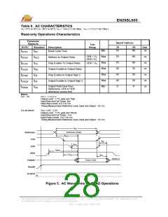
tRC
Addresses Stable
tACC
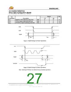
Addresses
CE#
tDF
tOE
OE#
tOEH
WE#
tCE
tOH
HIGH Z
Output Valid
Outputs
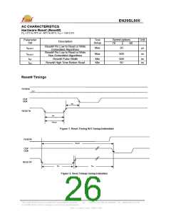
Reset#
RY/BY#
0V
Figure 5. AC Waveforms for READ Operations
This Data Sheet may be revised by subsequent versions
or modifications due to changes in technical specifications.
©2004 Eon Silicon Solution, Inc., www.essi.com.tw
28
Rev. D, Issue Date: 2006/11/06

 EON [ EON SILICON SOLUTION INC. ]