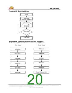
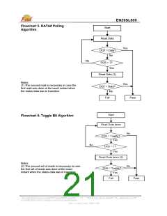
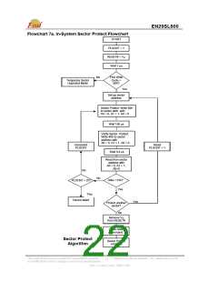
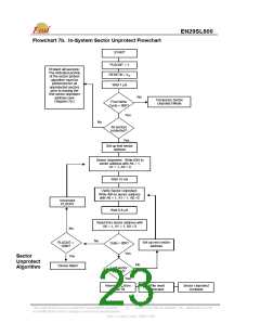
EN29SL800
Table 7. DC Characteristics
(Ta = 0°C to 70°C or - 40°C to 85°C; VCC = 1.65-2.2V)
Symbol
Parameter
Test Conditions
Min
Max
Unit
Typ
Input Leakage Current
Output Leakage Current
±3
±3
30
30
µA
µA
I
0V≤ V ≤ Vcc
IN
LI
I
0V≤ V
≤ Vcc
OUT
LO
Active Read Current (Byte mode)
Active Read Current (Word mode)
15
15
mA
mA
CE# = V , OE# = V
IL
,
IH
I
I
I
CC1
F=5MHz
CE# = BYTE# =
RESET# = Vcc
(Note 1)
CE# = BYTE# =
RESET# = Vcc
(Note 1)
Supply Current (Standby - CMOS)
VCC , Reset Current
0.2
0.2
5.0
5.0
µA
CC2
CC3
µA
Byte program, Sector or
Chip Erase in progress
15
30
mA
I
I
CC4
CC5
Supply Current (Program or Erase)
V
= Vcc ± 0.2 V
= Vss ± 0.2 V
IH
0.2
5.0
µA
V
Automatic Sleep Mode
Input Low Voltage
V
IL
0.3 x
VCC
Vcc +
0.3
-0.5
V
IL
0.7 x
Vcc
Input High Voltage
Output Low Voltage
V
V
V
V
IH
0.25
V
I
= 2.0 mA
= -2.0 mA
OL
OL
0.85 x
Vcc
Vcc -
0.4V
Output High Voltage TTL
I
OH
OH
V
OH
Output High Voltage CMOS
V
I
= -100 μA,
A9 Voltage (Electronic Signature)
A9 Current (Electronic Signature)
9.0
1.2
10.0
11.0
50
V
V
ID
A9 = VID
µA
I
ID
Supply voltage (Erase and
Program lock-out)
V
LKO
1.5
V
Notes
1. BYTE# pin can also be GND ± 0.3V. BYTE# and RESET# pin input buffers are always enabled so that
they draw power if not at full CMOS supply voltages.
This Data Sheet may be revised by subsequent versions
or modifications due to changes in technical specifications.
©2004 Eon Silicon Solution, Inc., www.essi.com.tw
24
Rev. D, Issue Date: 2006/11/06

 EON [ EON SILICON SOLUTION INC. ]