DA14580
FINAL
Bluetooth Low Energy 4.2 SoC
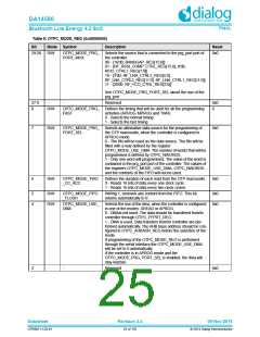
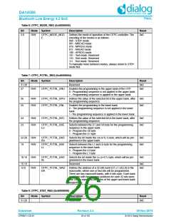
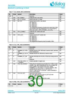
Table 6: OTPC_MODE_REG (0x40008000)
Bit
Mode Symbol
R/W OTPC_MODE_MOD
Description
Reset
2:0
Defines the mode of operation of the OTPC controller. The
encoding of the modes is as follows:
000 - STBY mode
0x0
E
001 - MREAD mode
010 - MPROG mode
011 - AREAD mode
100 - APROG mode
101 - Test mode. Reserved
110 - Test mode. Reserved
111 - Test mode. Reserved
To manually move between modes, always return to STBY
mode first.
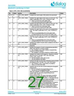
Table 7: OTPC_PCTRL_REG (0x40008004)
Bit
Mode Symbol
Description
Reset
0x0
31:28
27
-
-
Reserved
R/W
OTPC_PCTRL_ENU
Enables the programming in the upper bank of the OTP.
0 - Programming sequence is not applied in the upper bank.
1 - Programming sequence is applied in the upper bank.
0x0
26
25
R/W
R/W
OTPC_PCTRL_BITU
OTPC_PCTRL_ENL
Defines the value of the selected bit in the upper bank, after
the programming sequence.
0x0
0x0
Enables the programming in the lower bank.
0 - The programming sequence is not applied in the lower
bank.
1 -The programming sequence is applied in the lower bank.
24
23
R/W
R/W
OTPC_PCTRL_BITL
Defines the value of the selected bit in the lower bank, after
the programming sequence.
0x0
0x0
OTPC_PCTRL_BSE
LU
Selects between the U1 and U0 byte for the programming
sequence in the upper bank.
0 - Program the U0 byte
1 - Program the U1 byte
22:20
19
R/W
R/W
OTPC_PCTRL_BAD
RU
Selects the bit inside the Ux (x=0,1) byte, which will be pro-
grammed in the upper bank.
0x0
0x0
OTPC_PCTRL_BSE
LL
Selects between the L1 and L0 byte for the programming
sequence in the lower bank.
0 - Program the L0 byte
1 - Program the L1 byte
18:16
R/W
OTPC_PCTRL_BAD
RL
Selects the bit inside the Lx (x=0,1) byte, which will be pro-
grammed in the lower bank.
0x0
15:13
12:0
-
-
Reserved
0x0
0x0
R/W
OTPC_PCTRL_WAD
DR
Defines the address of a 32 bits word {U1,L1,U0,L0} in the
macrocells, where one or two bits will be programmed.
There are two macrocell banks, with 8 bits each. Each bank
contribute with two memory positions for each 32 bits word.
The Ux, Lx represent the bytes of the upper and lower bank
respectively.
Table 8: OTPC_STAT_REG (0x40008008)
Bit
Mode Symbol
Description
Reset
31:29
-
-
Reserved
0x0
Datasheet
Revision 3.4
09-Nov-2016
CFR0011-120-01
26 of 155
© 2014 Dialog Semiconductor

 DIALOG [ Dialog Semiconductor ]