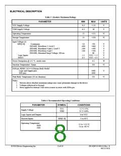
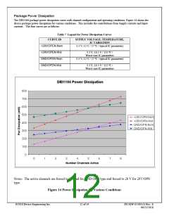
ELECTRICAL DESCRIPTION
Table 3 Absolute Maximum Ratings
PARAMETER
MIN
-0.3
-0.3
MAX
+5.0
18
UNITS
VCC Supply Voltage
VDD Supply Voltage
V
V
Operating Temperature
Storage Temperature
-55
-55
+125
+150
°C
°C
Input Voltage (3)
DIN[1:8]
Continuous
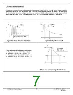
DO160E, Waveform 3, Level 3
DO160E, Waveform 4 and 5, Level 3
DO160E, Waveform 4 and 5
DO160E, Abnormal Surge Voltage, 100 ms
-10
+49
+600
+300
+500
80
V
V
V
V
V
V
V
-600
-300
-500
Logic Inputs
DOUT
-1.5
-0.5
VCC + 1.5
VCC + 0.5
Power Dissipation @ 125 °C, steady state
Junction Temperature, Tjmax
0.5
W
145
°C
ESD per JEDEC A114-A Human Body Model
Logic and Supply pins
2000
1000
V
DIN pins
Peak Body Temperature (10 sec duration)
235
°C
Notes:
1. Stresses above absolute maximum ratings may cause permanent damage to the device.
2. Voltages referenced to Ground
3. Stress applied to external 3 kΩ series resistor in series with DINn pin.
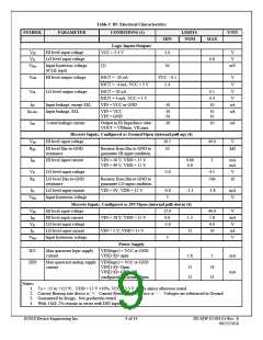
Table 4 Recommended Operating Conditions
PARAMETER
Supply Voltage
SYMBOL
CONDITIONS
VCC
VDD
3.3 V ±5%
15 V ±10%
Logic Inputs and Outputs
Discrete Inputs
0 to VCC
-3 to 49 V
DIN[1:8]
Ta
Operating Temperature
-55 to +125 ºC
-55 to +85 ºC
-SMS
-SES
©2018 Device Engineering Inc.
8 of 14
DS-MW-01184-01 Rev. E
06/25/2018

 DEIAZ [ Device Engineering Incorporated ]