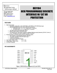
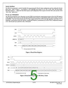
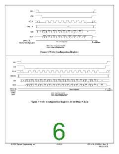
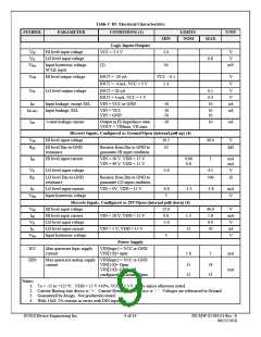
Serial Interface
The DEI1184 incorporates a serial IO interface for programming the Discrete Input configuration and for reading the Discrete
Input status. Refer to Figure 2. The interface is SPI compatible and consists of /CS, SEL, SCLK, SDO, and SDI signals.
Waveform Figures 4 – 7 depict the Data Read sequence and Configuration Write sequence for both 8-Bit cycles and also 16 bit
“daisy chain” applications.
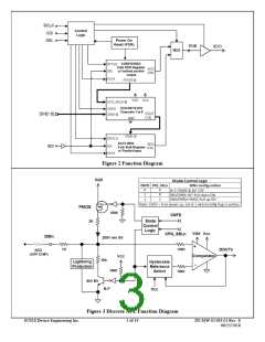
Power Up Initialization
The DEI1184 incorporates an on-chip power-on reset (POR) circuit and power sequencing provisions to force the DIN inputs to
a high impedance state at power up; the AFE pull-up (PMOS switch in Figure 3) and pull-down (BJT switch in Figure 3) circuits
are disabled. The reset circuit monitors the VCC logic supply and forces the AFE to the high impedance state while VCC is
stabilizing. It will remain in this state until the Configuration Register is programmed by the first Write Configuration Register
cycle, when the pull-up or pull-down state is determined.
SEL
/CS
X
SCLK
X
VALID
X
X
DIN[1:8]
X
X
SDI
SDO
DIN8
DIN7
DIN6
DIN5
DIN4
DIN3
DIN2
DIN1
DIN inputs latched into DATA S-Reg
Figure 4 Read Data Register
SEL
/CS
X
SCLK
X
VALID
X
X
DIN[1:8]
SI8
SI7
SI6
SI5
SI4
SI3
SI2
SI1
X
X
SDI
DIN8
DIN7
DIN6
DIN5
DIN4
DIN3
DIN2
DIN1
SI8
Si7
SI6
SI5
SI4
SI3
SI2
SI1
SDO
DIN inputs latched into DATA S-Reg
SDI data shifted to SDO after 8 bit delay
Figure 5 Read Data Register, 16 Bit Daisy Chain
©2018 Device Engineering Inc.
5 of 14
DS-MW-01184-01 Rev. E
06/25/2018

 DEIAZ [ Device Engineering Incorporated ]