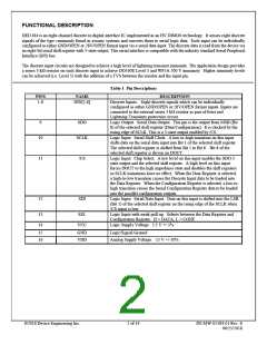
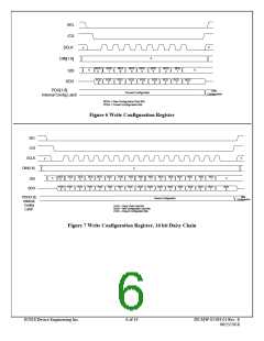
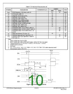
SEL
/CS
X
SCLK
X
X
DIN[1:8]
NCD
8
NCD
7
NCD
6
NCD
5
NCD
4
NCD
3
NCD
2
NCD
1
X
X
SDI
PCD
8
PCD
7
PCD
6
PCD
5
PCD
4
PCD
3
PCD
2
PCD
1
NCD
8
SDO
PDO[1:8]
Internal Config Latch
New
Configuration
Present Configuration
NCDn = New Configuration Data Bits
PCDn = Present Configuration Bits
Figure 6 Write Configuration Register
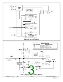
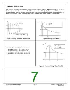
SEL
/CS
X
SCLK
X
X
DIN[1:8]
DCD
8
DCD
7
DCD
6
DCD
5
DCD
4
DCD
3
DCD
2
DCD
1
NCD
8
NCD
7
NCD
6
NCD
5
NCD
4
NCD
3
NCD
2
NCD
1
X
X
SDI
PCD
8
PCD
7
PCD
6
PCD
5
PCD
4
PCD
3
PCD
2
PCD
1
DCD
8
DCD
7
DCD
6
DCD
5
DCD
4
DCD
3
DCD
2
DCD
1
NCD
8
SDO
New
Configuration
PDO[1:8]
Internal
Config
Latch
Present Configuration
DCDn = Daisy Chain Data Bits
NCDn = New Configuration Data Bits
PCDn = Present Configuration Bits
Figure 7 Write Configuration Register, 16 bit Daisy Chain
©2018 Device Engineering Inc.
6 of 14
DS-MW-01184-01 Rev. E
06/25/2018

 DEIAZ [ Device Engineering Incorporated ]