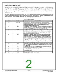
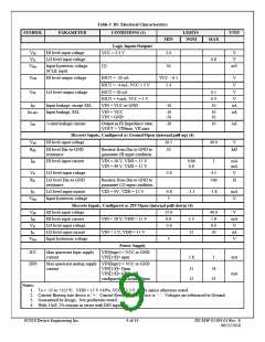
Table 2 Truth Table
Serial Interface Operation
SEL
X
H
/CS SCLK
SDI
X
X
DIN[1:8]
SDO
HI Z
DIN[8]
DR[8]
Description
Not Selected
DR[1:8]← DIN[1:8]
H
↓
X
L
↑
X
Valid
X
H
L
DR[1]
DR[n+1] ← DR[n], DR[1] ← SDI
L
L
L
↑
↑
L
CR[1]
X
X
X
CR[8]
HI Z
CR[n+1] ← CR[n], CR[1] ← SDI
CL[1:8]← CR[1:8]
Legend:
DR = Data Register
CR = Configuration Register
CL = Configuration Latch
X = Don’t Care
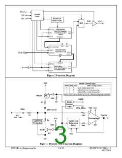
DIN[1:8] Discrete AFE
The Discrete Input Analog Front End circuit function is represented in Figure 3. Each DINn signal is conditioned by the resistor
/ diode network and presented to a comparator with hysteresis. The external 3 kΩ resistor is part of the front-end circuitry for
achieving threshold and hysteresis requirements while protecting the chip from Lightning Induced Transients. When the input is
configured for GND/OPEN operation (By programming the channel’s configuration register bit to 1), the pull-up resistor and
diode is enabled by turning PMOS switch on and BJT switch off. The comparator reference voltage corresponding to DINn
input threshold (shown below) is generated from resistive network. When configured for 28V/OPEN operation, the pull-down
resistor is enabled by turning BJT on and PMOS off. The comparator reference voltages for 28V/OPEN operation are configured
corresponding to DINn input threshold voltages described below.
Some notable features are:
·
·
The input current is ~1 mA. This current will prevent a “dry” relay contact.
The input threshold voltage and hysteresis:
o
o
28V/OPEN
·
·
·
Low- level input voltage:
High level input voltage:
Hysteresis:
-3.0 V to 6.0 V
12 V to 49 V
Vhys > 3V
GND/OPEN
·
·
·
Low- level input voltage:
High level input voltage:
Hysteresis:
-3.0 V to 4.5 V
10.5 V to 49 V
Vhys > 3 V
·
·
Input noise immunity is maximized with a combination of voltage hysteresis and use of a slow input voltage comparator.
The inputs can withstand continuous input voltages of 49 V. The isolation diode breakdown voltage is greater than
42V. The 10 kΩ input resistance, which consists of a 7 kΩ on-chip resistor and a 3 kΩ off-chip resistor, is designed to
limit diode breakdown current to safe levels during transient events.
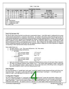
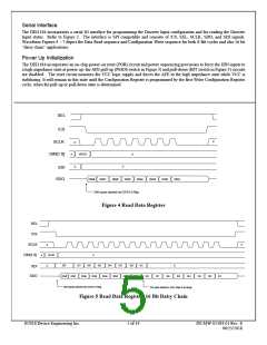
Data Register
The 8-bit Data Register is a “parallel-input, serial-output” register that samples the input channels and reads-out the data to the
Serial Data Output. The register is read via the SDO output as described in Figure 4 and Figure 5. A low DIN input level
results in a Logic 0, and a high input level results in a Logic 1.
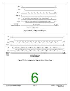
Configuration Register
The 8-bit Configuration Register is a “serial-input, parallel-output with data latch” register that individually configures each
AFE input as either GND/OPEN or 28V/OPEN format. The register is programmed via the serial data input as described in
Figure 6 and Figure 7. Logic 0 sets the respective input to 28V/OPEN mode (pull-down); Logic 1 sets the respective input to
GND/OPEN mode (pull-up). The register is reset to 0’s when the VCC Logic Supply voltage transitions from low to high.
©2018 Device Engineering Inc.
4 of 14
DS-MW-01184-01 Rev. E
06/25/2018

 DEIAZ [ Device Engineering Incorporated ]