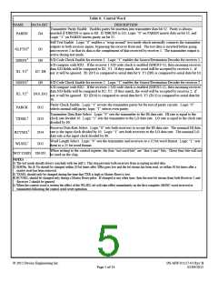
Power-Up Reset
Power-up reset and Master Reset:
An internal power-up reset circuit prevents erroneous data
transmission before an external master reset has been applied.
The user must apply an active Lo pulse to the Master Reset pin
(/MR) after power up or upon system reset. Preceding the master
reset at power-up an internal power-up reset occurs which will
clear the transmitter such that no erroneous serial data stream will
be transmitted before master reset. Receivers, control register, and
internal control logic are reset by master reset.
TX Word Gap Timer
The TX word gap timer circuit inserts a 4 bit time gap between
words. This gives a minimum requirement of a 29 bit time or a 36
bit time for each word transmission. The 4 bit time gap is also
automatically maintained when the next new block of data is
loaded into the buffer, which may take less than one bit time.
After resetting the device, the user must program the control
register before beginning normal operation. The control register
may be reprogrammed without additional reset pulses.
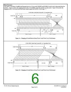
25-bit Word Operation:
The TRANSCEIVER implements a 25 bit word format which
may be used in non-ARINC applications to enhance data transfer
rate. The format is a simplified version of the 32 bit ARINC word
and is described in Figure 3. It consists of an 8 bit label, a 16 bit
data word, and a parity bit. The parity bit can optionally be
replaced with a 17th data bit. The Source/Destination code
checking option can be enabled in either receiver. It will operate
on bits 9 and 10 of the 25 bit word.
Serial Interface:
The DEI1116/1117 consists of two receive channels and one
transmit channel.
Each receive channel operates
independently of each other and the transmitter. The receive
data is asynchronous to the transmitter data and can also be at
a different data rate than the transmitter.
Transmitter
The transmitter clock is free running and in phase with the
transmitter data. The transmitter data (DO(A) and DO(B)) are
TTL level signals. There are always at least 4 null bits
between data words. An external ARINC line driver is
required to interface the transmitter to the ARINC serial data
bus. See ARINC 429 LINE DRIVERS below.
Self-Test Operation:
By selecting the control register bit (/SLFTST) self test option,
the user may perform a functional test of the TRANSCEIVER
and support circuitry. The user can write data into the transmitter
and it will be internally wrapped around into both receivers. The
user can then verify reception and integrity of the data. The
receiver line interface and the user's line drivers will not be tested.
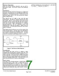
Receiver
By setting the transmitter to use even parity, the user can test the
receiver's parity circuit operation.
The receiver signals (DI(A) and DI(B)) are differential,
bipolar, return-to-zero logic signals. The ARINC channels
can be connected directly to the receiver with no external
components on the DEI1116. The DEI1117 requires external
10K ohm series resistors.
Processor Interface:
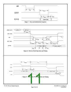
Figure 7 shows a typical reset and initialization sequence. The
user must pulse the /MR pin low to reset the device. To load the
Control Register from the data bus, the /LDCW pin is pulsed low
while the desired control data is applied on the data bus.
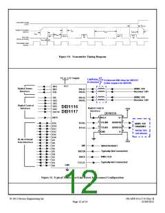
ARINC 429 Line Driver
Device Engineering offers a complete line of ARINC line
drivers ICs that support the ARINC 429, 571, and 575
standards. Refer to DEI website at: http://www.deiaz.com.
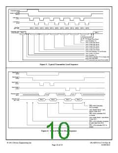
Figure 5 shows a typical transmitter loading sequence. It begins
with the transmitter completing transmission of the previous data
block. The TXR flag goes HI to notify the user that data may be
loaded into the buffer. The user sets ENTX to LO to disable the
Transmitter and proceeds to load a total of six ARINC words into
the buffer. (Note that up to eight words could have been loaded).
The user then enables the transmitter by setting ENTX to a logic
"1" and the transmitter begins it's sequence of sending out data
words. Although not shown in the figure, the transmitter loading
sequence can be interrupted by receiver reading cycle with no
interference between the two operations.
Figure 6 shows a typical receiver reading sequence. Both
receivers notify the user of valid data ready by setting their
respective /DRn lines to logic "0". The user responds by first
reading the two data words from Receiver 1 and then from
Receiver 2. The SEL line is normally a system address line and
may assume any state, but must be valid when the /OEn line is
pulsed low.
© 2012 Device Engineering Inc.
DS-MW-01117-01 Rev B
02/09/2012
Page 9 of 14

 DEIAZ [ Device Engineering Incorporated ]