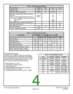
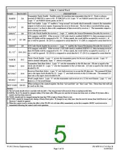
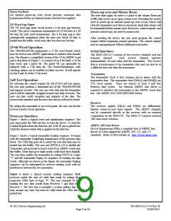
Table 6: Control Word
DESCRIPTION
NAME
PAREN
DATA BIT
D4
Transmitter Parity Enable. Enables parity bit insertion into transmitter data bit 32. Parity is always
inserted if /DBCEN is open or HI. If /DBCEN is LO, Logic “0” on PAREN inserts data on bit 32, and
Logic “1” on PAREN inserts parity on bit 32.
Self Test Enable. Logic “0” enables a “wrap around” test mode which internally connects the transmitter
outputs to both receiver inputs, bypassing the receiver front end. The test data is inverted before going
into receiver 2 so that its data is the complement of that received by receiver 1. The transmitter output is
active during test mode.
/SLFTST1
SDEN12
X1, Y12
SDEN22
X2, Y22
D5
D6
S/D Code Check Enable for receiver 1. Logic “1” enables the Source/Destination Decoder for receiver 1.
S/D compare code RX1. If the receiver 1 S/D code check is enabled (SDEN1=1), then incoming receiver
data S/D fields will be compared to X1, Y1. If they match, the word will be accepted by receiver 1; if
not, it will be ignored. X1 (D7) is compared to serial data bit 9, Y1 (D8) is compared to serial data bit 10.
D7, D8
D9
S/D Code Check Enable for receiver 2. Logic “1” enables the Source/Destination Decoder for receiver 2.
S/D compare code RX2. If the receiver 2 S/D code check is enabled (SDEN2=1), then incoming receiver
data S/D fields will be compared to X2, Y2. If they match, the word will be accepted by receiver 2; if
not, it will be ignored. X2 (D10) is compared to serial data bit 9, Y2 (D11) is compared to serial data bit
10.
D10, D11
Parity Check Enable. Logic “1” inverts the transmitter parity bit for test of parity circuits. Logic “0”
PARCK
TXSEL3
D12
D13
selects normal odd parity; logic “1” selects even parity.
Transmitter Data Rate Select. Logic “0” sets the transmitter to the HI data rate. HI rate is equal to the
clock rate divided 10. Logic “1” sets the transmitter to the LO data rate. LO rate is equal to the clock rate
divided by 80.
Receiver Data Rate Select. Logic “0” sets both receivers to accept the HI data rate. The nominal HI data
rate is the input clock divided by 10. Logic “1” sets both receivers to the LO data rate. The nominal LO
data rate is the input clock divided by 80.
RCVSEL4
WLSEL5
D14
D15
Word Length Select. Logic “0” sets the transmitter and receivers to a 32 bit word format. Logic “1” sets
them to a 25 bit word format.
When writing to the control register, the four “not used bits” are “don’t care” bits. These four bits will not
be used on the chip.
NOT USED D0-D3
NOTES
1) The test mode should always conclude with ten null’s. This step prevents both receivers from accepting invalid data.
2) SDENn, Xn & Yn should be changed within 20 bit times after /DRn goes low and the bit stream has been read, or within 30 bit times after a
master reset has been removed.
3) TXSEL should only be changed during the time that TXR is high or Master Reset is low.
4) RCVSEL should be changed only during a Master Reset pulse. If changed at any other time, then the next bit stream from both Receiver 1 and
Receiver 2 should be ignored.
5) When the control word is written the effect of the WLSEL bit will take effect immediately on the first complete ARINC word received or
transmitted following the control word write operation.
© 2012 Device Engineering Inc.
DS-MW-01117-01 Rev B
02/09/2012
Page 5 of 14

 DEIAZ [ Device Engineering Incorporated ]