and Word 2 together have an even number of 1’s, then data bit
32 is a logic “1”. Otherwise, it is a logic “0”.
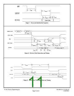
Receiver Operation:
Since the receivers function identically, only one will be
discussed in detail. The receiver consists of the following
circuits.
Line Receiver
The front end of the Line Receiver functions as a voltage level
translator. It transforms the ±10 volt differential ARINC data
signals into 5 Volt internal logic levels. The line receivers are
protected against shorts to ±40 Volts and provide common
mode voltage rejection.
The DEI1116 and 1117 differ in their A429 RX input
characteristics. The DEI1116 interfaces directly to the A429
bus signals. DEI1117 version bypasses some of the on-chip
resistance and thus operates with 10K ohm series resistors.
The series resistors support implementation of lightning
transient protection. The 1117 withstands Level 3 pin
injection levels with only the resistors. Higher levels are
achieved with a TVS shunt placed between the series resistor
and 1117 DIxx pin.
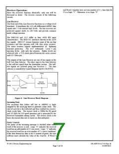
The outputs of the Line Receiver are one of two inputs to the
Self-Test Data Selector. The other input to the Data Selector
is the self-test signal from the transmitter section. The self-
test signals are inverted going into Receiver 2. The data
selector is controled by Control Register bit D5 (/SLFTST).
DO(A)
DI1(A)
Self-Test
To
Data Selector
Receive
DI1(B)
Decoder
Comparator
SLFTST
Figure 4: Line Receiver Block Diagram
Incoming Data
The incoming data (either self test or ARINC) is triple
sampled by the word gap timer to generate a data clock. The
start of each bit is first detected and then verified two receive-
clock cycles later. The receive clock is 1MHz for HI speed
and 125 KHz for LO speed operation and is generated by the
Receiver/Transmitter timing circuit. The receive clock is ten
times the normal data rate to ensure no data ambiguity.
Parity Control
The parity of the incoming message is checked when either
word of the receiver is read. Logic “0” indicates the received
word has an odd number of 1’s (no error). Logic “1” indicates
the received word has an even number of 1’s (error condition).
If the data format has data in bit 32 instead of parity, the user
software must calculate the value of the 32nd bit. If Word 1
© 2012 Device Engineering Inc.
DS-MW-01117-01 Rev B
02/09/2012
Page 7 of 14

 DEIAZ [ Device Engineering Incorporated ]