PDF
最近搜索
热门搜索
发布采购

| 型号: | DEI1117-QMS-G |
| PDF下载: | 下载PDF文件 查看货源 |
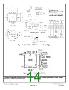
| 内容描述: | [Transceiver Family] |
| 分类和应用: | 驱动接口集成电路驱动器 |
| 文件页数/大小: | 14 页 / 587 K |
| 品牌: |  DEIAZ [ Device Engineering Incorporated ] DEIAZ [ Device Engineering Incorporated ] |
专业IC领域供求交易平台:提供全面的IC Datasheet资料和资讯,Datasheet 1000万数据,IC品牌1000多家。