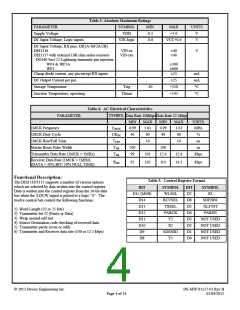
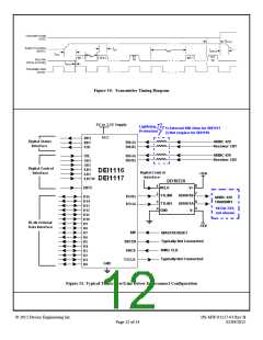
S/D Decoder
Transmitter Operation:
The Source/Destination decoder compares the user set code (X
and Y) with bits 9 and 10 of the data word. The decoder can
be enabled and disabled by the SDENn bits of the Control
Register. If the two codes are matched, a signal is generated
to latch in the received data into the receiver buffer.
Otherwise the data word is ignored and not latched into the
receive buffer. If the data is latched, the data ready flag
(/DRn) is set to indicate to the user that a valid data word is
ready to be read.
The transmitter section consists of an 8 word by 32 bit FIFO,
parity generator, transmitter word gap timer, and a TTL output
circuit.
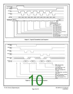
FIFO Buffer
The 8x32 buffer memory allows the user to load up to 8 words
into the transmitter, enable it, and then ignore it while the
transmitter ships out the data without further attention. Data is
loaded into the buffer by pulsing /LD1 to load the first 16 bits
(WORD 1) from the data bus, and pulsing /LD2 to load WORD
2. /LD1 must always precede /LD2. The transmitter must always
be disabled while loading the buffer (ENTX = logic "0").
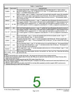
Data Clock
The derived data clock then shifts the data down a 32 bit long
Data Shift Register. The data word length is selectable for
either 25 or 32 bits long by Control Register Bit WLSEL. As
soon as the data word is completely received, an internal
signal is generated by the word gap timer circuit to enable
loading data into the 32 bit receive buffer latch.
If the buffer is full and new data is pulsed with /LD1 and /LD2,
the last 32 bit word in the buffer will be overwritten. Data will
remain in the buffer until ENTX is pulsed to a logic “1”, which
will activate the FIFO clock and data is shifted out serially to the
transmitter driver.
Data Access
The buffer data is transmitted until the last word in the buffer is
shifted out. At this time a transmitter ready signal (TXR) is set to
a logic “1” indicating that the buffer is empty and ready to receive
up to eight more data words. Writing into the buffer memory is
disabled when ENTX is set to logic “1”.
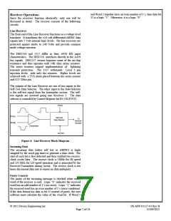
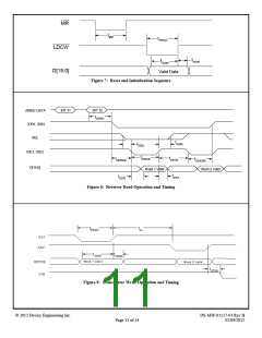
To access the receiver data, the user sets the receiver data
select input (SEL) to a logic “0” and pulses the output enable
(/OEn) line with a logic “0”. This causes Data Word 1 to be
placed on the 16 bit data bus. To read Word 2, the user sets
the data select input (SEL) to a logic “1” and pulses the output
enable (/OEn) low to place Word 2 on the data bus. When
both Word 1 and Word 2 have been read, DRn will be reset.
This reset is triggered by the leading edge of the final /OEn
pulse.
Transmitter Ready Signal (TXR)
The transmitter ready flag (TXR) is set to logic “0” with the first
occurrence of an /LD2 pulse to indicate that the buffer is not
empty.
If a new data word is received before the previous data has
been read from the receiver buffer (as indicated by the /DRn
signal flip-flop), the receive buffer will not be over written by
the new data. The new data will remain in the shift register
until either the /DRn signal is reset and it can be written into
the receive buffer or it is overwritten by the next incoming
data word. Data in the shift register will be overwritten by
new incoming data, while data that has been latched into the
receive buffer can not be overwritten.
Output Register
The output register is designed such that it can shift out a word of
25 bits or 32 bits. The length is controlled by control register bit
"WLSEL".
Parity Generator
The parity generator calculates either odd or even parity as
specified by control register bit "PARCK". Odd parity is normally
used; even parity is available to test the receiver parity check
circuit. Odd parity means that there is an odd number of 1's in the
25 or 32 bit serial word. Bit 8 of word one is replaced with a
parity bit if parity is selected by the control register bit "PAREN"
and the /DBCEN pin. Otherwise, bit 8 is passed through as data.
Data Error Conditions
If the receiver input data word string is broken before the
entire data word is received, the receiver will reset and ignore
the partially received data word.
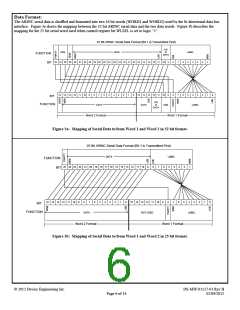
Transmitter Output
The transmitter driver outputs three TTL compatible signals: 1)
DO(A), 2) DO(B), and 3) TXCLK. DO(A) and DO(B) are the
transmitter data in two rail, return-to-zero format. DO(A)
indicates a logic "1" data bit by going to a "1" for the 1st half of a
bit time, then returning to "0" for the 2nd half; DO(B) remains at
"0" for the whole bit time. In the same fashion, DO(B) indicates a
logic "0" data bit by pulsing HI while DO(A) remains LO. A null
bit is indicated when both signals remain LO. It is illegal for both
signals to be logic "1". The TXCLK is a free running clock signal
of 50% duty cycle and in phase with transmitter data. The clock
will always be logic "1" during the first half of a bit time.
If the receiver input data word string is not properly framed
with at least 1 null bit before the word and 1 null bit after the
word, the receiver will reset and ignore the improperly framed
data word.
© 2012 Device Engineering Inc.
DS-MW-01117-01 Rev B
02/09/2012
Page 8 of 14

 DEIAZ [ Device Engineering Incorporated ]