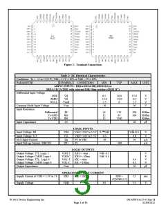
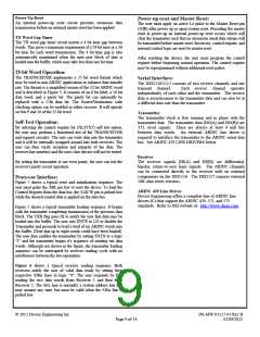
Table 3: Absolute Maximum Ratings
PARAMETER
Supply Voltage
DC Input Voltage, Logic inputs
SYMBOL
VDD
VIN-logic
MIN
-0.5
-0.6
MAX
+7.0
VCC+0.6
UNITS
V
V
DC Input Voltage, RX pins: DI[1A/1B/2A/2B]
DEI1116
VIN-rx
±40
±40
V
DEI1117 with external 10K ohm series resistors
VIN-rxe
DO160 Sect 22 Lightning Immunity pin injection
WF4 & WF5A
±300
±600
WF3
Clamp diode current, any pin except RX inputs
DC Output Current per pin
Storage Temperature
±25
±25
+150
+145
mA
mA
°C
Tstg
-65
Junction Temperature, operating
TJmax
°C
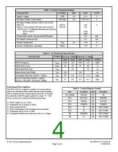
Table 4: AC Electrical Characteristics
SYMBOL
PARAMETER
1MCK Frequency
1MCK Duty Cycle
1MCK Rise/Fall Time
Data Rate 100kbpsData Rate 12.5kbps
MIN
0.99
40
MAX
1.01
60
MIN
0.99
40
MAX
1.01
60
UNITS
MHz
%
ns
ns
kbps
f1MCK
CKDC
TCRF
TMR
10
10
Master Reset Pulse Width
Transmitter Data Rate (1MCK = 1MHz)
200
99
200
12.4
TDR
101
105
12.6
14.5
Receiver Data Rate (1MCK = 1MHz),
RDR
95
8.0
kbps
(DATA = 50% BIT/ 50% NULL TIME)
Functional Description:
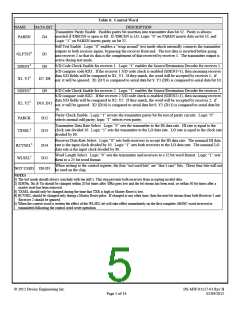
Table 5: Control Register Format
The DEI1116/1117 supports a number of various options
which are selected by data written into the control register.
Data is written into the control register from the 16-bit data
bus when the /LDCW signal is pulsed to a logic “0”. The
twelve control bits control the following functions:
BIT
SYMBOL
WLSEL
RCVSEL
TXSEL
PARCK
Y2
BIT
D7
D6
D5
D4
D3
D2
D1
D0
SYMBOL
X1
SDENB1
/SLFTST
PAREN
NOT USED
NOT USED
NOT USED
NOT USED
D15 (MSB)
D14
D13
D12
D11
D10
D9
D8
1) Word Length (32 or 25 bits)
2) Transmitter bit 32 (Parity or Data)
3) Wrap around self test.
4) Source Destination code checking of received data.
5) Transmitter parity (even or odd)
X2
6) Transmitter and Receiver data rate (100 or 12.5 kbps)
SDENB2
Y1
© 2012 Device Engineering Inc.
DS-MW-01117-01 Rev B
02/09/2012
Page 4 of 14

 DEIAZ [ Device Engineering Incorporated ]