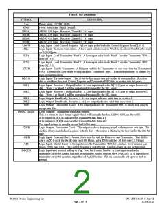
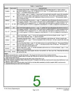
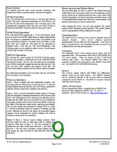
Table 1: Pin Definitions
DEFINITION
SYMBOL
VDD
GND
Power Input. +5VDC ±10%
Power Return and Signal Ground.
DI1(A)
DI1(B)
DI2(A)
DI2(B)
/LDCW
SEL
ARINC 429 Input. Receiver Channel 1, “A” input
ARINC 429 Input. Receiver Channel 1, “B” input
ARINC 429 Input. Receiver Channel 2, “A” input
ARINC 429 Input. Receiver Channel 2, “B” input
Logic Input. Load Control Register. A Low input pulse loads the Control Register from D[15:0].
Logic Input. Receiver word select. A Low input selects receiver Word 1; Hi selects Word 2 to be read
on D [15:0] port.
/LD1
/LD2
Logic Input. Load Transmitter Word 1. A Low input pulse loads Word 1 into the Transmitter FIFO
from D [15:0].
Logic Input. Load Transmitter Word 2. A Low input pulse loads Word 2 into the Transmitter FIFO
from D [15:0].
ENTX
Logic Input. Enable Transmitter. A Hi input enables the Transmitter to send data from the Transmitter
FIFO. This must be Low while writing data into Transmitter FIFO. Transmitter memory is cleared by
high-to-low transition.
D[15:0]
/OE1
Logic Input / Tri-state Output. This 16-bit bi-directional data port is the uP data interface. Receiver
data is read from this port. Control Register and Transmitter FIFO data is written into this port.
Logic Input. Receiver 1 Output Enable. A Low input enables the D [15:0] port to output Receiver 1
data. Word 1 or Word 2 will be output as determined by the SEL input.
/OE2
Logic Input. Receiver 2 Output Enable. A Low input enables the D [15:0] port to output Receiver 2
data. Word 1 or Word 2 will be output as determined by the SEL input.
/DR1
/DR2
TXR
Logic Output. Data Ready, Receiver 1. A Low output indicates valid data in receiver 1.
Logic Output. Data Ready, Receiver 2. A Low output indicates valid data in receiver 2.
Logic Output. Transmitter Ready. A Hi output indicates the Transmitter FIFO is empty and ready to
accept new data.
DO(A), DO(B)
Logic Outputs. Transmitter serial data outputs.
This is a return-to-zero format signal which will normally feed an ARINC 429 Line Driver IC.
A Hi output on DO(A) indicates the Transmitter data bit is a 1.
A Hi output on DO(B) indicates the Transmitter data bit is a 0.
The signal returns to zero for second half of bit time.
TXCK
Logic Output. Transmitter Clock. This outputs a clock frequency equal to the transmit data rate. The
clock is always enabled and in phase with the data. The output is Hi during the first half of the data bit
time.
1MCK
/MR
Logic Input. External Clock. Master clock used by both the Receivers and Transmitter. The 1MHz
rate is an X10 clock for the HI data rate (100 kbps), and a X80 clock for LO data rate (12.5 kbps).
Logic Input. Master Reset. A Lo input resets the Transmitter FIFO, bit counters, word counter, gap
timers, /DRx, and TXR. The Control Register is not affected. Used on power up and system reset.
/DBCEN
Logic Input with internal pull up to VDD. Data Bit Control Enable. A Low input enables the
transmitter parity bit control function as defined by control register bit 4 (PAREN). A Hi input forces
transmitter parity bit insertion regardless of PAREN value. The pin is normally left open or tied to
ground.
© 2012 Device Engineering Inc.
DS-MW-01117-01 Rev B
02/09/2012
Page 2 of 14

 DEIAZ [ Device Engineering Incorporated ]