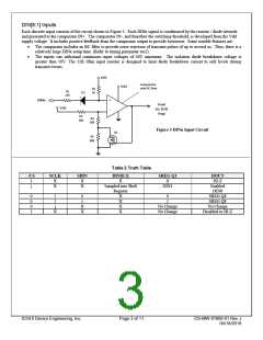
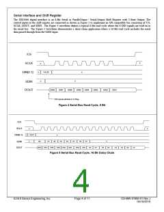
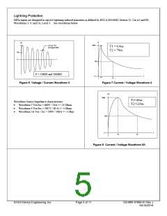
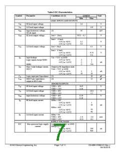
Symbol
Parameter
Conditions (1) (2)
LIMITS
Min Max
Unit
IDD
Max quiescent analog
supply current
Logic Inputs = VCC or GND
DIN[8:1] = Open
11
DIN[8:1] = GND
mA
23
24
-55°C to +85°C
-55°C to +125°C
Notes:
1. Unless otherwise noted, Ta = rated temperature range. VCC = 3.0 to 5.5V. VDD = 5.0 to 18V.
2. Current flowing into device is positive. Current flowing out of device is negative. Voltages are
referenced to Ground.
3. By design, not tested.
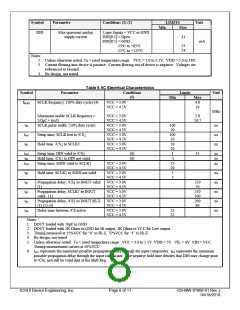
Table 6 AC Electrical Characteristics
Symbol
Parameter
Conditions
(5)
Limits
Unit
Min
Max
fMAX
SCLK frequency. (50% duty cycle) (4)
VCC = 3.0V
VCC = 4.5V
4.8
24
MHz
Maximum usable SCLK frequency =
1/(tp2 + tsu3)
SCLK pulse width. (50% duty cycle)
VCC = 3.0V
VCC = 4.5V
VCC = 3.0V
VCC = 4.5V
VCC = 3.0V
VCC = 4.5V
VCC = 3.0V
VCC = 4.5V
2.8
10.7
tW
tsu1
th1
100
20
100
50
20
20
1
ns
ns
ns
Setup time, SCLK low to /CS↓.
Hold time, /CS↓ to SCLK↑.
tsu2
th2
tsu3
Setup time, DIN valid to /CS↓.
Hold time, /CS↓ to DIN not valid.
Setup time, SDIN valid to SCLK↑.
(6)
(6)
35
us
us
ns
-1
VCC = 3.0V
VCC = 4.5V
VCC = 3.0V
VCC = 4.5V
75
20
5
th3
tp1
tp2
tp3
tp4
Hold time, SCLK↑ to SDIN not valid.
ns
ns
ns
ns
ns
5
Propagation delay, /CS↓ to DOUT valid. VCC = 3.0V
250
70
250
100
200
80
(1)
VCC = 4.5V
VCC = 3.0V
VCC = 4.5V
Propagation delay, SCLK↑ to DOUT
valid. (1)
Propagation delay, /CS↑ to DOUT HI-Z. VCC = 3.0V
(1) (2) (3)
Delay time between /CS active.
VCC = 4.5V
VCC = 3.0V
VCC = 4.5V
25
25
Notes:
1. DOUT loaded with 50pF to GND.
2. DOUT loaded with 1K Ohms to GND for Hi output, 1K Ohms to VCC for Low output.
3. Timing measured at 25%VCC for “0” to Hi-Z, 75%VCC for “1” to Hi-Z.
4. By design, not tested
5. Unless otherwise noted: Ta = rated temperature range. VCC = 3.0 to 5.5V. VDD = 5V. VIL = 0V. VIH = VCC.
Timing measurement cursers at 50%VCC.
6. tsu2 represents the maximum possible propagation delay through the input comparator. th2 represents the minimum
possible propagation delay through the input comparator. The negative hold time denotes that DIN may change prior
to /CS↓ and still be valid data at the Shift Reg.
©2018 Device Engineering, Inc.
Page 8 of 11
DS-MW-01066-01 Rev J
04/18/2018

 DEIAZ [ Device Engineering Incorporated ]