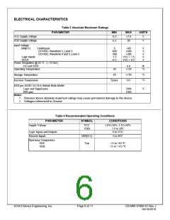
ELECTRICAL CHARACTERISTICS
Table 3 Absolute Maximum Ratings
PARAMETER
MIN
-0.3
-0.3
MAX
+7.0
20
UNITS
VCC Supply Voltage
VDD Supply Voltage
V
V
Input Voltage
DIN[8:1]
Continuous
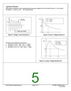
DO160D, Waveform 3, Level 3
DO160D, Waveform 4 and 5, Level 3
-5
+40
+600
+300
V
V
V
V
V
-600
-300
-1.5
-0.5
Logic Inputs
DOUT
VCC + 1.5
VCC + 0.5
Power Dissipation @ 85 °C: (> 10 Sec)
16 Lead SOIC
0.8
W
Operating Temperature
-55
-65
+125
°C
+150
°C
°C
Storage Temperature
Junction Temperature
Tjmax
145
ESD per JEDEC A114-A Human Body Model
Logic and Supply pins
DIN pins
2000
1000
V
Notes:
1. Stresses above absolute maximum ratings may cause permanent damage to the device.
2. Voltages referenced to Ground
Table 4 Recommended Operating Conditions
PARAMETER
Supply Voltage
SYMBOL
CONDITIONS
VCC
VDD
5.0V±10%, 3.3V±10%
5.0 to 18V
Logic Inputs and Outputs
Discrete Inputs
0 to VCC
DIN[8:1]
Top
0 to 40V
Operating Temperature
-SES
-SMx
-55 to +85 ºC
-55 to +125 ºC
©2018 Device Engineering, Inc.
Page 6 of 11
DS-MW-01066-01 Rev J
04/18/2018

 DEIAZ [ Device Engineering Incorporated ]