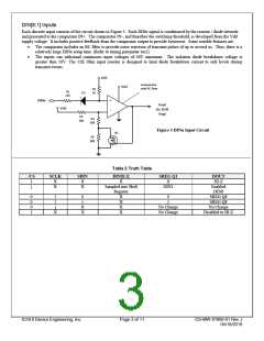
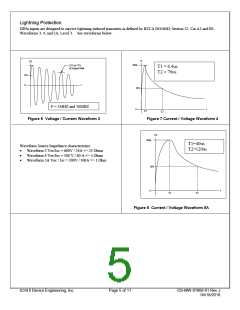
DIN[8:1] Inputs
Each discrete input consists of the circuit shown in Figure 3. Each DINn signal is conditioned by the resistor / diode network
and presented to the comparator IN+. The comparator IN-, and therefore the switching threshold, is developed from the Vdd
supply voltage. It includes positive feedback from the comparator output to provide hysteresis. Some notable features are:
·
The comparator includes an RC filter to provide noise rejection of transient pulses of up to several us. Thus, there is a
relatively large DINx setup time. (Refer to timing parameter tsu2).
·
The inputs can withstand continuous input voltages of 40V minimum. The isolation diode breakdown voltage is
greater than 50V. The 12K Ohm input resistor is designed to limit diode breakdown current to safe levels during
transient events.
Vdd
Comparator
Vdd
with RC filter
R2
3K
R1
12K
D1
+
-
DINn
Vout
(to Shift
Reg)
Vdd
R3
500
R4
50K
Figure 3 DINn Input Circuit
Q1
R5
80K
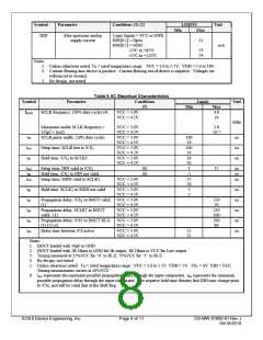
Table 2 Truth Table
/CS
1
↓
SCLK
X
X
SDIN
X
X
DIN[8:1]
SREG Q1
X
DIN1
DOUT
HI-Z
Enabled
DIN8
X
Sampled into Shift
Register
0
0
0
↑
↑
↑
↓
0
1
X
X
X
X
X
X
0
1
SREG Q8
SREG Q8
No Change
No Change
No Change
X
Disabled to HI-Z
©2018 Device Engineering, Inc.
Page 3 of 11
DS-MW-01066-01 Rev J
04/18/2018

 DEIAZ [ Device Engineering Incorporated ]