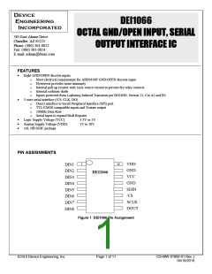
GENERAL DESCRIPTION
The DEI1066 is an eight-channel discrete-to digital interface BICMOS device. It senses eight Ground/Open discrete signals of
the type commonly found in avionic systems. The data is read from the device via an eight-bit serial shift register with 3-state
output implemented as a Serial Peripheral Interface (SPI) bus, Mode 0 slave.
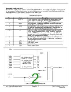
Table 1 Pin Descriptions
Pins
Name
Description
8-1
DIN[8:1]
Parallel data inputs. Eight Ground/Open format discrete signals. These
have an internal pull-up to VDD. The logic threshold and hysteresis
characteristics are determined by the applied VDD voltage.
Serial data output. This pin is the output from the last stage of the shift
register. This is a 3-state output.
Serial Shift Clock. A low-to-high transition on this input shifts data on
the serial data input into the shift register and data in stage 8 is shifted out
DOUT, being replaced by the data previously stored in stage 7.
Chip Select. A high-to-low transition on this input loads data from the
parallel DIN[8:1] inputs into the shift register. A low level on this input
enables the DOUT 3-state output and the shift register. A high level on
this input forces DOUT to the high impedance state and disables the shift
register so SCLK transitions have no effect.
9
DOUT
SCLK
10
11
12
/CS
SDIN
Serial Data Input. Data on this input is shifted into the shift register on
the rising edge of the SCLK input if the /CS input is low. This input has
an internal pull-down resistor to GND.
13
14
15
16
GND
VCC
GND
VDD
Logic Ground.
Logic Supply Voltage.
Analog Ground.
Analog Supply Voltage.
SDIN
SDIN
DI1
DI2
DI3
DI4
DI5
DI6
DI7
DI8
DIN1
DIN2
DIN3
DIN4
DIN5
DIN6
DIN7
DIN8
INPUT RESISTORS,
COMPARATORS,
FILTERING, AND
LIGHTNING
PROTECTION
(8 CHANNELS)
Q8
DOUT
SHIFT REG
SCK
SCLK
/CS
SH/LD
Figure 2 DEI1066 LOGIC DIAGRAM
©2018 Device Engineering, Inc.
Page 2 of 11
DS-MW-01066-01 Rev J
04/18/2018

 DEIAZ [ Device Engineering Incorporated ]