DS3251/DS3252/DS3253/DS3254
Early Termination of Bus Transactions. The bus master can terminate SPI bus transactions at any time by
pulling CS high. In response to early terminations, the DS325x resets its SPI interface logic and waits for the start
of the next transaction. If a write transaction is terminated prior to the SCLK edge that latches the LSB of a data
byte, the current data byte is not written.
Design Option: Wiring SDI and SDO Together. Because communication between the bus master and the
DS325x is half-duplex, the SDI and SDO pins can be wired together externally to reduce wire count. To support
this option, the bus master must not drive the SDI/SDO line when the DS325x is transmitting.
AC Timing. See Table 17-I and Figure 17-5 for AC timing specifications for the SPI interface.
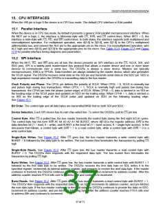
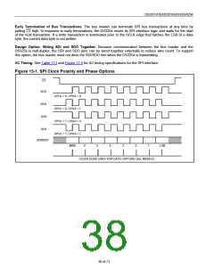
Figure 15-1. SPI Clock Polarity and Phase Options
CS
SCK
CPOL = 0, CPHA = 0
SCK
CPOL = 0, CPHA = 1
SCK
CPOL = 1, CPHA = 0
SCK
CPOL = 1, CPHA = 1
SDI/SDO
MSB
6
5
4
3
2
1
LSB
CLOCK EDGE USED FOR DATA CAPTURE (ALL MODES)
38 of 71

 DALLAS [ DALLAS SEMICONDUCTOR ]