DS3251/DS3252/DS3253/DS3254
15. CPU INTERFACES
When the HW pin is logic 0 the device is in CPU bus mode. The default CPU interface is 8-bit parallel.
15.1 Parallel Interface
When the device is in CPU bus mode, by default it presents a generic 8-bit parallel microprocessor interface. When
the MOT pin is logic 1, the interface is Motorola-style with CS, R/W, and DS control lines. When MOT = 0, the
interface is Intel-style with CS, RD, and WR control lines. In both styles, the interface supports both multiplexed and
nonmultiplexed operation. For multiplexed operation, wire A[5:0] to D[5:0], wire D[7:0] to the CPU’s multiplexed
address/data bus, and connect the ALE pin to the appropriate pin on the micro. For nonmultiplexed operation, wire
ALE high and wire A[5:0] and D[7:0] to the appropriate pins on the micro. See Table 17-H, Figure 17-3 and Figure
17-4 for parallel interface timing diagrams and parameters.
15.2 SPI Interface
When the MOT, RD, and WR pins are all low, the device presents an SPI interface on the CS, SCLK, SDI, and
SDO pins. SPI is a widely-used master/slave bus protocol that allows a master device and one or more slave
devices to communicate over a serial bus. The DS325x is always a slave device. Masters are typically
microprocessors, ASICs or FPGAs. Data transfers are always initiated by the master device, which also generates
the SCLK signal. The DS325x receives serial data on the SDI pin and transmits serial data on the SDO pin. SDO is
high-impedance except when the DS325x is transmitting data to the bus master.
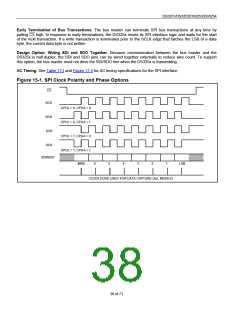
Clock Polarity and Phase. The CPOL pin defines the polarity of SCLK. When CPOL = 0, SCLK is normally low
and pulses high during bus transactions. When CPOL = 1, SCLK is normally high and pulses low during bus
transactions. the CPHA pin sets the phase (active edge) of SCLK. When CPHA = 0, data is latched in on SDI on
the leading edge of the SCLK pulse and updated on SDO on the trailing edge. When CPHA = 1, data is latched in
on SDI on the trailing edge of the SCLK pulse and updated on SDO on the following leading edge.
See Figure 15-1.
Bit Order. The control byte and all data bytes are transmitted MSB first on both SDI and SDO.
Device Selection. Each SPI device has its own chip-select line. To select the DS325x, pull its CS pin low.
Control Byte. After CS is pulled low, the bus master transmits the control byte during the first eight SCLK cycles.
The control byte has the form R/W A5 A4 A3 A2 A1 A0 BURST, where A[5:0] is the register address, R/W is the
data direction bit (1 = read, 0 = write), and BURST is the burst bit (1 = burst access, 0 = single-byte access). In the
discussion that follows, a control byte with R/W = 1 is a read control byte, while a control byte with R/W = 0 is a
write control byte.
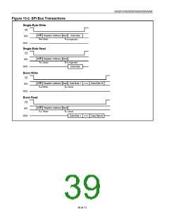
Single-Byte Writes. See Figure 15-2. After CS goes low, the bus master transmits a write control byte with
BURST = 0 followed by the data byte to be written. The bus master then terminates the transaction by pulling CS
high.
Single-Byte Reads. See Figure 15-2. After CS goes low, the bus master transmits a read control byte with
BURST = 0. The DS325x then responds with the requested data byte. The bus master then terminates the
transaction by pulling CS high.
Burst Writes. See Figure 15-2. After CS goes low, the bus master transmits a write control byte with BURST = 1
followed by the first data byte to be written. The DS325x receives the first data byte on SDI, writes it to the
specified register, increments its internal address register, and prepares to receive the next data byte. If the master
continues to transmit, the DS325x continues to write the data received and increment its address counter. After the
address counter reaches FFh it rolls over to address 00h and continues to increment.
Burst Reads. See Figure 15-2. After CS goes low, the bus master transmits a read control byte with BURST = 1.
The DS325x then responds with the requested data byte on SDO, increments its address counter, and pre-fetches
the next data byte. If the bus master continues to demand data, the DS325x continues to provide the data on SDO,
increment its address counter, and pre-fetch the following byte. After the address counter reaches FFh it rolls over
to address 00h and continues to increment.
37 of 71

 DALLAS [ DALLAS SEMICONDUCTOR ]