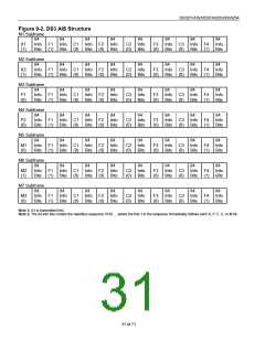
DS3251/DS3252/DS3253/DS3254
12. CLOCK ADAPTER
The clock adapter block generates all required clock rates from a single input clock. If a transmission-quality clock
of one line rate (DS3, E3 or STS-1) is present, the clock adapter can synthesize transmission-quality clocks at the
other two line rates. Both input clocks and synthesized clocks are then available to be used as master clocks by the
CDRs and jitter attenuators. In hardware mode the clock adapter is entirely controlled by the T3MCLK, E3MCLK
and STMCLK pins. See the pins descriptions for those pins in Table 6-A.
In CPU bus mode additional clock adapter control options are available in the CACR register. When control bit
AMCEN is set to 1, the clock adapter block is configured for alternate master clock mode. In this mode, the clock
adapter expects to receive a clock whose frequency is specified by the AMCSEL[1:0] control bits rather than a
DS3, E3 or STS-1 clock. Valid input frequencies are 19.44 MHz, 38.88 MHz and 77.76 MHz. In alternate master
clock mode the clock adapter can synthesize up to two clock rates (DS3, E3 or STS-1). To synthesize DS3 and E3
clocks, the alternate master clock should be applied to the STMCLK pin. To synthesize DS3 and STS-1 clocks, the
clock should be applied to the E3MCLK pin. To synthesize E3 and STS-1 clocks, the clock should be applied to the
T3MCLK pin. The device can be powered up with an alternate clock applied to one of the MCLK pins, even though
the power-on default values of AMCEN and AMCSEL[1:0] may not match the applied clock. Once these control bits
are properly set after power-up, the clock adapter begins to synthesize the proper master clocks, and the device as
a whole functions normally.
CPU bus mode also provides the ability to output synthesized master clocks on the T3MCLK, E3MCLK and
STMCLK pins for use by neighboring framers, mappers and other components. To output the synthesized DS3
master clock on T3MCLK, set CACR:T3MOE=1. To output the synthesized E3 master clock on E3MCLK, set
CACR:E3MOE=1. To output the synthesized STS-1 master clock on STMCLK, set CACR:STMOE=1.
13. RESET LOGIC
There are four sources for reset: an internal power-on reset (POR) circuit, the reset pin RST, the JTAG reset pin
JTRST, and the RST bit in each LIU’s global configuration register (GCR). The chip is divided into three zones for
reset: the digital logic, the analog circuits, and the JTAG logic. The digital logic includes the status and control
registers, the B3ZS/HDB3 encoder and decoder, the PRBS generator and detector, and the LOS detect logic. The
analog circuits include clock and data recovery, jitter attenuator, and transmit waveform generation. The JTAG
logic consists of the common boundary scan controller and the boundary scan cells at each pin.
The POR circuit resets the digital logic, analog circuits, and JTAG logic zones. The RST pin resets the digital logic
and the analog circuits but not the JTAG logic. The JTRST pin resets only the JTAG logic. Each LIU’s RST register
bit resets the digital logic for that LIU, including resetting the LIU’s registers to the default state (except for the RST
bit itself).
The POR signal and RST pin require an active master clock source for the LIU to properly reset.
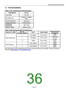
35 of 71

 DALLAS [ DALLAS SEMICONDUCTOR ]